Our Techniques
Home » Our Techniques
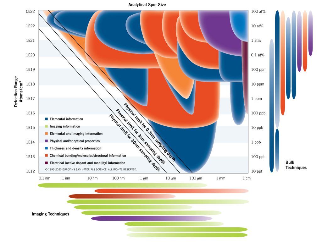
The EAG SMART (Spectroscopy and Microscopy Analytical Resolution Tool) Chart shown below offers a concise visual reference for comparing analytical techniques. Easily compare the detection limits and analytical resolutions of dozens of techniques used for materials characterization, evaluation surface analysis, purity surveys and more. Select a technique to learn more or contact an EAG Scientist. Download a printable version of this chart or view our SMART Chart Webinar series.
Scroll to the bottom of this page to view a list of all our in-house techniques.

/EELS
Nanometer scale elemental identification and mapping with TEM and STEM
/EDS
Elemental composition of small areas with a 1-2 nm range using STEM imaging
Quantitative elemental analysis of samples with small surface areas
/EDS
Elemental composition of small areas with a 0.1-3 μm range using SEM imaging
Ideal for qualitative analysis of organic, inorganic and mixed materials
/ESCA
Surface analysis technique to determine quantitative atomic composition and chemistry
Non-destructive technique for characterization of crystalline materials
Precise thin film thickness and optical constants measurements
Determination of thickness, interface roughness and density for thin films and multilayers
Quick identification of complex mixtures of materials and further characterization
Non-destructive elemental analysis for film thickness and composition measurements
Quantitative compositional thin film analysis without reference standards
H
E
M
Depth profiling for electrical properties including carrier concentration and mobility
Probe
3D atom map, element distribution and nanoscale structure characterization
NanoIR combines AFM with infrared spectroscopy
High-resolution digital cathodoluminescene (CL) images of luminescent materials
Characterize relative element abundances and element distribution in any solid sample
Surface microanalysis at ppm range and near complete characterization of materials
ICPMS
High precision elemental and stable isotope analysis of solid materials
Highly surface-sensitive technique for analyzing surface metal contamination
Unrivaled capabilities in SIMS analysis for dopant and impurity detection
Chemical analysis and characterization at the nano scale with great spatial resolution
Visualization of microstructure with spatial coordinates of crystalline samples
Provides visualization of material phase, crystal structure and stain level at nanometer (nm) scale
High-resolution surface topography images with elemental microanalysis and particle characterization
3D topographic imaging for surface roughness quantification and further characterization
High-resolution cross-section images of samples for SEM, STEM and TEM analysis
Mechanical characterization of highly-localized material properties
SEM-based technique for semiconductor failure analysis and device characterization
Surface topography characterization for a wide range of sample geometries and dimensions
Non-destructive, real time inspection of electronic components and metallurgical samples
D
M
S
Direct analysis of chemical composition and trace/ultra-trace level determinations
V
T
C
P
Quantitative chemical analysis with high sensitivity for a wide range of elements
C
High-throughput, versatile technique for charged molecule analysis
C
M
S
Identify and quantify organic compounds in mixtures with low detection limits
C
M
S
Identification, quantitation and mass analysis of materials in a complex matrix
G
A
Measure gas-forming elements (C, H, O, N and S) in solids from ppm to percentage levels
G
A
Thermal stability and degradation measurements from physical and chemical changes
S
C
Thermal analytical tool for best processing temperatures, sample composition and quality
M
R
Chemical structure and composition analysis with quantitative information
P
C
Characterization of polymers and other macromolecules in mixtures

Technique List
Would you like to learn more about our techniques?
Contact us today for your technical needs. Please complete the form below to have an EAG expert contact you.