FIB Circuit Edit & Debug
Home » Services » Microelectronics Test & Engineering » FIB Circuit Edit & Debug
Focused Ion Beam, or FIB circuit edit, services allow the customer to cut traces or add metal connections within a chip. Our services include sample preparation, sample analysis, fault isolation and actual circuit modifications. These circuit edits could support basic electrical design characterization or verification of redesign parameters. Our full range of debug tools enables you to solve even the most vexing logic failures and other anomalies.
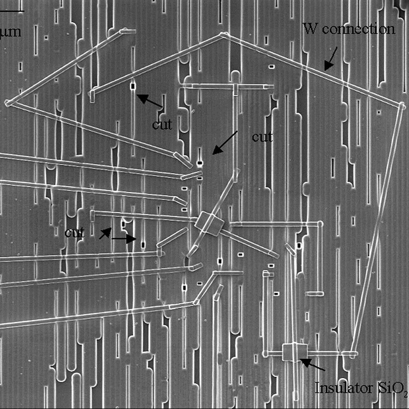
FIB circuit edit employs a finely focused Ga+ ion beam to image, etch and deposit materials on an integrated circuit. The beam’s 4-5 nm resolution allows for extremely precise edits to be made. The FIB is coupled to a navigation system (Knights/Camelot/Lavis) providing a method to find subsurface features and ensuring that the right edits are made. The high energy Ga beam can mill through conductors and, by utilizing the appropriate gas chemistries, tungsten, platinum or silicon dioxide can be precisely deposited using the ion beam.
Focused ion beam circuit edits can be done quickly and easily, at a small fraction of the cost of a new lot of wafers in a fab. Circuit edits are often performed once a design flaw has been identified to ensure that the proposed fix will solve the complete problem.
With our state-of-the-art equipment and specialized techniques, we can edit circuits at advanced process nodes such as 28 nm, 20 nm and 14 nm with multiple layer metal stacks, as well as back side editing for flip chip packages. Our electronics engineers have many years of experience throughout Silicon Valley and have the knowledge and capability necessary to accommodate the most demanding requests. FIB edits often require rapid turnaround and cannot afford mistakes – our years of experience and focus on customer satisfaction make EAG the smart choice in circuit editing.
FIB Circuit Edit processes
EAG’s FIB circuit edit services include the following processes, all of which can be performed with approximately 20 nm accuracy:
- Metal deposition
- Dielectric deposition
- Metal and dielectric etch, including material-specific chemical etch enhancement
- Imaging of the device using the incident ion beam
These capabilities allow FIB to perform some key functions:
- Circuit edit by connecting and cutting signal lines in order to modify the logic of circuitry
- Probe pad formation at specific locations by exposing the desired trace and connecting to a newly formed probe pad
- Increase or decrease resistance in a circuit
- Failure analysis: FIB Passive Voltage Contrast (PVC) defect localization is more sensitive and more reproducible than the corresponding SEM. When an interesting feature is observed, the FIB is capable of providing additional information to help determine root cause.
- The defective region can be marked in the FIB for further characterization
- The defect can be cross-sectioned and imaged in the FIB
- The defect can be isolated by cutting the appropriate adjacent circuit components
FIB Circuit Edit Beyond 20nm
Many experts in our industry believe that Circuit Edit using a Focused Ion Beam is no longer feasible for process nodes below 20 nm. EAG Laboratories has been able to assist our customers with Circuit Edits on geometries at the single digit nanometer scale. With the rising cost of the development of devices at advanced nodes reaching over $10 million, this Application Note will discuss the typical uses and how our engineers push the limits of this technique to allow early correction of any device errors, and also allow for the ability to generate hundreds of edited samples for customer demonstrations, and continued development and engineering test.
Would you like to learn more about FIB Circuit Edit & Debug?
Contact us today for your FIB Circuit Edit & Debug needs. Please complete the form below to have an EAG expert contact you.