2D/3D realtime X-ray inspection solutions
As components get more complex, nondestructive inspection techniques like X-Ray and CT scanning help uncover issues and anomalies
Home » Microelectronics Testing

As components get more complex, nondestructive inspection techniques like X-Ray and CT scanning help uncover issues and anomalies
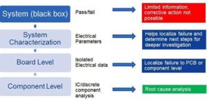
Electronic systems failure analysis methodology and workflow by applying FIB circuit edit techniques for solving electronic problems.
ATE testing automates and streamlines the testing process of microelectronic devices by using specialized hardware and software to perform a wide range of functional tests under various conditions. Come learn more about ATE and what EAG can do for you.

Damage caused by ESD is one of the primary failure mechanisms for integrated circuits. Testing susceptibility to ESD events is crucial in the success of electronic devices and is essential for the qualification process.
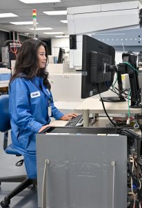
Our wide range of ATE test equipment and experienced team can support from first silicon debug to release

In sectors like the automotive industry, ATE plays a pivotal role in verifying the proper and reliable operation of critical systems.
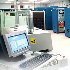
Our world class labs can provide you with all the reliability qualification you need

Aerospace and defense government suppliers can have confidence in EAG’s credibility in providing accurate and high-quality testing services.
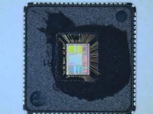
Chemical Decapsulation: Creation of a cavity on the package surface of an electronic component to expose the die underneath for inspection.
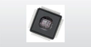
In this webinar we introduce Microelectronic Component Product Qualification to understand and consider component reliability.
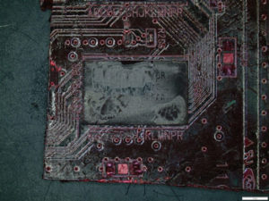
Dye and Pry is an excellent way to inspect a large number of bonds (leads, solder ball, seals..) at one time

In this webinar we introduce Dye and Pry that involves cleaning a sample to remove debris & flux around solder, then exposing it to a red dye.
19th December 2019
EAG Laboratories is proud to help the Global Semiconductor Alliance incubation team assist semiconductor startups
15th May 2015
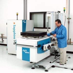
Electronics failure analysis services from EAG extended with millions in new tool investments, adding latest precision imaging and inspection equipment.
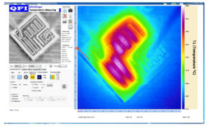
QFI Instrument Services and electrical localization services from EAG Laboratories are upgraded with LSM and XIVA image.
In this webinar we introduce failure analysis of ICs and other components in the product development cycle and for improving current products
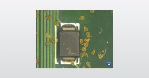
In this webinar we introduce Environmental chamber clean analysis that identifies contamination that can ruin your qualifications.
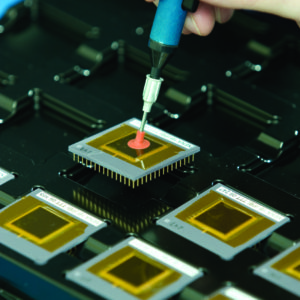
Our highly experienced team utilizes the most up-to-date testing methodologies for the most accurate results

In this webinar we introduce electrostatic discharge (ESD) testing which is one of the failure mechanisms for integrated circuit parts

In this webinar we show how EAG troubleshoots electronic system failures using a multidisciplinary approach
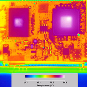
Expert failure analysis will shorten development cycles.
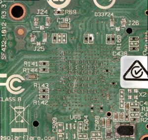
With in-depth images and analyses, EAG is able to examine the root cause of failures, critical dimensions, and quality of assembly process. Our experts can assist in PCB improvement.
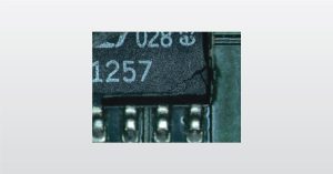
In this webinar we introduce The Failure Analysis of Reliability Testing Samples as applied electronic and semiconductor devices
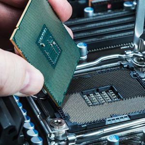
Failure inspection during post reliability stress testing to ensure no delamination, voids, cracks, material density changes.
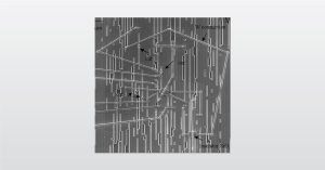
Speed up your product development cycle with quick and easy FIB edits
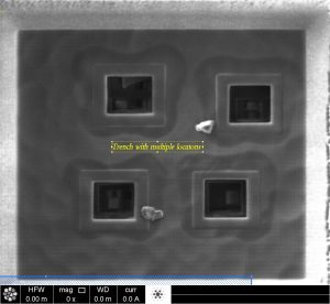
FIB Circuit Edit provides the ability to quickly perform nano-surgury by cutting traces or adding metal connections at the chip level

In this webinar we introduce FIB Circuit Edit which allows the cutting of connections and placement of new lines in a semiconductor die
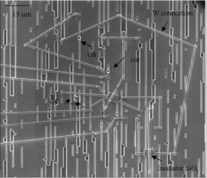
Focused Ion Beam (FIB) circuit edit techniques and FIB applications to help develop and improve IC design and advanced process nodes

High reliability electronic components like integrated circuits are often required to operate for long periods of time, having little or no opportunity for replacement.
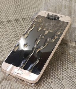
The type and degree of ingress protection that an enclosure possesses is described by the Ingress Protection (IP) rating.
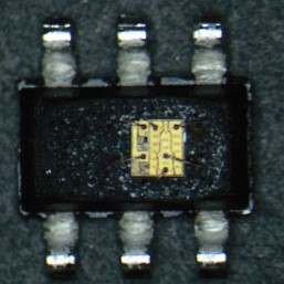
Laser decap at EAG Laboratories includes our Failure Analysis Laser Inspection Tool, view our picture book of PC boards before and after.
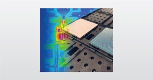
In this webinar we introduce latch-up testing which is relevant for CMOS devices with high static power dissipation.

LED characterization, from process control to failure analysis to construction analysis, EAG Laboratories supports your LED analysis needs.

Level 1 Failure Analysis includes: non-destructive tests optical inspection, X-ray, C-SAM, and electrical characterization.
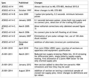
HBM ESD testing (Human Body Model electrostatic Discharge) uses the latest standards and best testing practices, reducing costs and time.

In this webinar we introduce Accelerated Life Testing and Failure Analysis techniques at EAG Laboratories Eindhoven
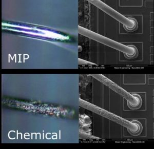
Microwave-Induced-Plasma (MIP) decapsulation allows for damage free removal of the protective cover of semiconductor packages.

Developing a reliable product has many challenges due to the desire for increased capability, reduction in formfactor, and managing the supply chain.
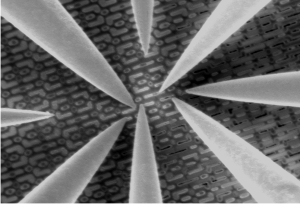
Nanoprobing is crucial for understanding advanced semiconductor devices, finding faults, and conducting thorough failure analysis.

EAG provides essential services for common devices and platforms that are instrumental to the electronics industry. These include artificial intelligence, ASICs, PCB Assembly, and Discretes.

EAG has success executing burn-in programs for new product qualifications to conducting Early-Life Failure Rate studies.
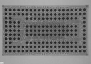
Package Delayering services helps to look for opens, shorts, leakage and damage in the layers and design rule distances in the sample.

Solving CSP qualification testing challenges by addressing key issues and applying specialized processes through EAG know-how.
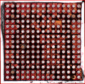
The common method of dye & pry can result in the cracking and shattering of die. EAG has altered the common dye & pry method, which has resulted in a significantly improved success rate.
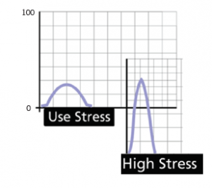
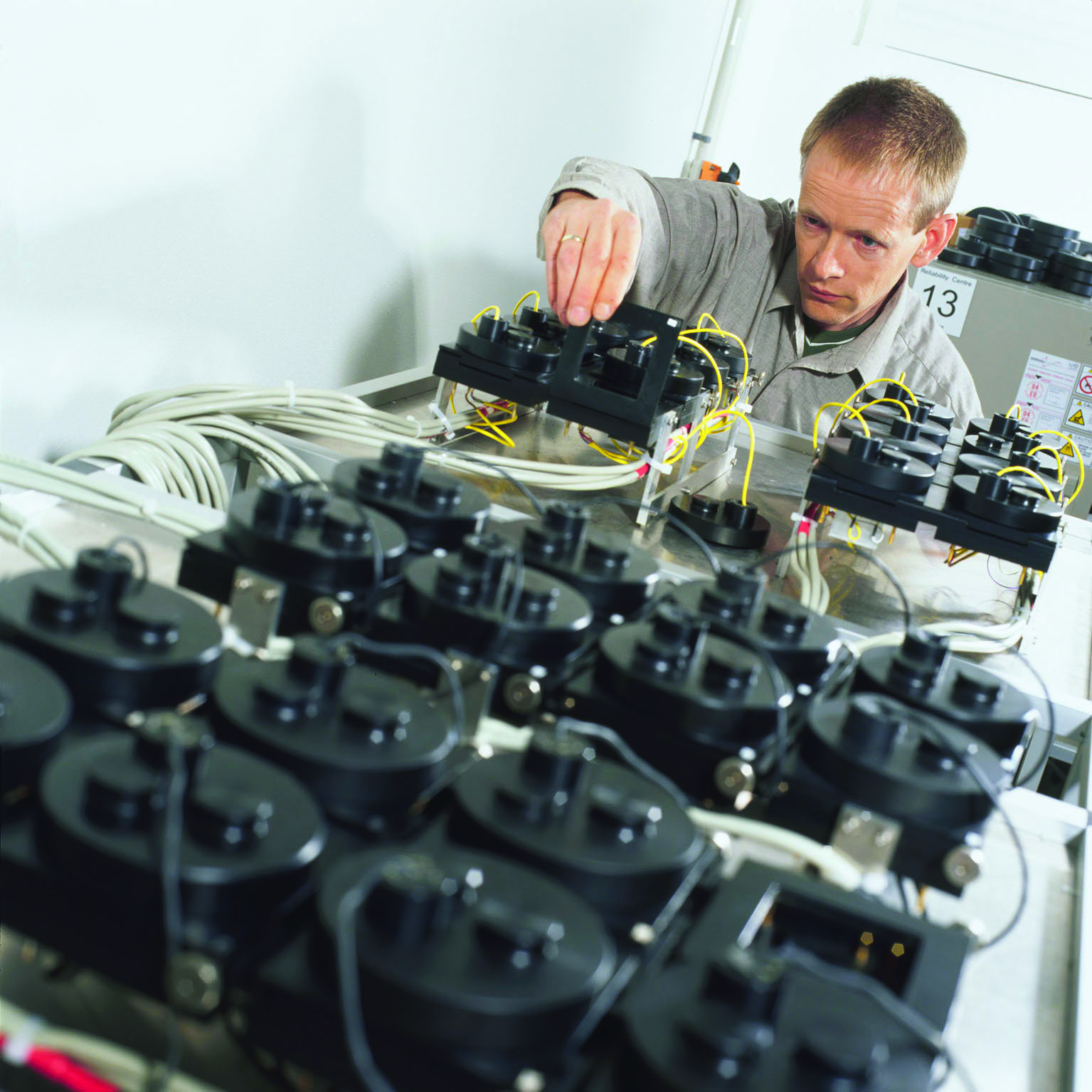
EAG has established product reliability test processes. In this example we inspect a Bluetooth speaker using Accelerated Testing.
Wednesday, March 26, 2025
In this webinar, we will show you how Eurofins EAG supports you in the various phases of reliability testing to come to a robust product, including the different types of actual testing.
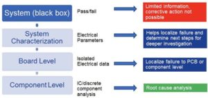
Electronic system failure analysis requires expertise in the modes of failures and techniques such as SEM, TEM, and dual-beam FIB.

In this webinar we introduce setting up reliability test plans, processing reliability data and the relation to the lifetime of a product

We help technology innovators translate ideas into realities, improve processes and products, and protect their brands

Through multidisciplinary science and engineering, EAG helps companies translate ideas into technology by supporting R&D, NPI and production.
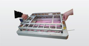
In this webinar we introduce the Testing of High Speed I/O to validate the devices from characterization to production
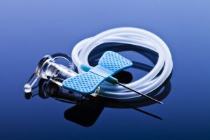
Failure analysis plays a crucial role in the development and maintenance of medical device electronics.
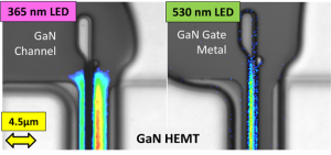
Eurofins EAG Laboratories has recently enhanced its thermal imaging capabilities with the integration of Microsanj equipment.
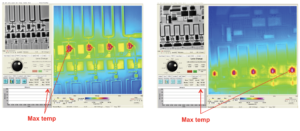
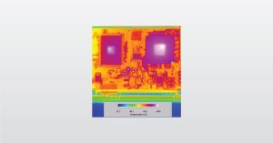
Temperature measurements of RF transistors to examine temperature distribution and look for areas of heating issues on many types of devices.
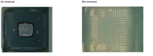
Time Domain Reflectometry (TDR) services from EAG – Each layer in the package may be inspected optically and probed electrically.
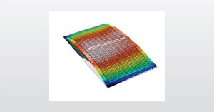
In this webinar we introduce Warpage and Strain Characterization used for non-contact, full-field acquisition of 3D topographies.
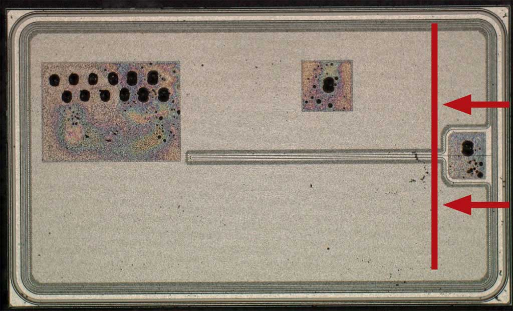
Cross sectioning of a semiconductor die is a basic step in failure analysis work. A cross section can be used as a check of layer integrity.
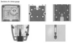
X-ray images from EAG include PCB layers, PC Board views, QFN, PCB Vias, QFP, Flip Chip, 9V Battery, BGA and BGA tilt and rotate.
To enable certain features and improve your experience with us, this site stores cookies on your computer. Please click Continue to provide your authorization and permanently remove this message.
To find out more, please see our privacy policy.