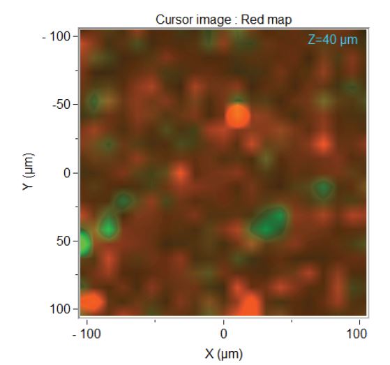
3D Confocal Raman Imaging of Pharmaceutical Creams and Tablets
A very good use of Raman is for the analysis of pharmaceutical products to determine the spatial distribution of components of interest
Home » Raman

A very good use of Raman is for the analysis of pharmaceutical products to determine the spatial distribution of components of interest
FTIR, Raman and NanoIR are particularly well suited at determining the identity and molecular structure of organic materials, however they can also obtain some inorganic information too.
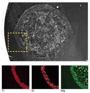
The chemical imaging of drug products helps to understand location/distribution of organic & inorganic constituents for formulation and IP

November 2, 2023
Please join us for coffee and conversations! Enjoy a cup of coffee and pastries as you get to know our technical experts.

February 15, 2024
Please join us for coffee and conversations! Enjoy a cup of coffee and pastries as you get to know our technical experts.
Essentials of Particulate Testing: USP <788> and AAMI TIR42 While there are many standards available for particulate testing, USP <788> and AAMI TIR42 are the

In this webinar we will focus on Fourier transform infrared (FTIR) and Raman spectroscopies comparing the two techniques

FTIR and Raman are spectroscopy techniques that provide molecular information from various types of materials.
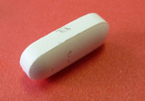
SEM-EDS and RAMAN analytical testing laboratory techniques applied to identification of foreign material contamination on pharmaceuticals.
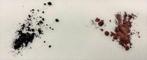
This paper describes identification of two unknown powders using Raman spectroscopy, combined with two X-ray techniques
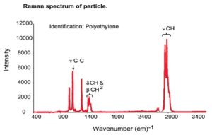
Learning the chemical composition of contaminants is challenging with small organic particles – Raman Spectroscopy is often the best approach
Battery characterization improves lithium-ion battery safety and performance using techniques such as SEM, TEM, XPS, GDMS, FTIR, ICP-OES, Raman and failure analysis
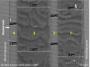
Understanding the construction/composition of films is beneficial for a variety of reasons
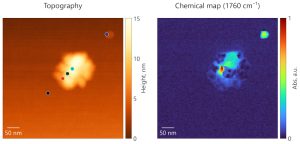
19th December 2022
EAG Laboratories is pleased to announce a new addition to our wide range of analytical techniques. Early next year, we’ll be offering NanoIR capabilities!
Semiconductor stress measurements by Raman Spectroscopy helps control problems related to stress control in semiconductor devices, from EAG.
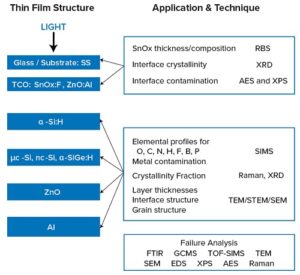
Surface analysis lab techniques on α-Si thin film PV, microcrystalline Si, nanocrystalline Si, amorphous SiGe, & microcrystalline SiC
Contamination control and defect reduction are critical issues in the manufacturing process of compound semiconductor devices which can impact the performance of the end product. We can provide valuable insights to identify contaminants and characterize materials throughout the product lifecycle.
To enable certain features and improve your experience with us, this site stores cookies on your computer. Please click Continue to provide your authorization and permanently remove this message.
To find out more, please see our privacy policy.