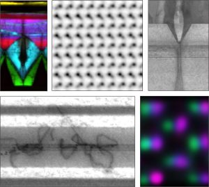
Advanced Microscopy of Compound Semiconductors
In this webinar, we will explore the variety of microscopy techniques available at Eurofins EAG commonly utilized to characterize compound semiconductor materials.
Home » Compound Semiconductors

In this webinar, we will explore the variety of microscopy techniques available at Eurofins EAG commonly utilized to characterize compound semiconductor materials.

Gallium oxide has the potential to replace or substitute gallium nitride for power conversion in electric trains and vehicles.

Aerospace Materials Testing for Tunnel Junction Solar Cells Science has opened many doors in its advancement over the centuries.
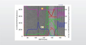
In the full webinar we will focus on the PCOR-SIMS Analysis of GaAs pHEMT and GaN HEMT using Secondary Ion Mass Spectrometry
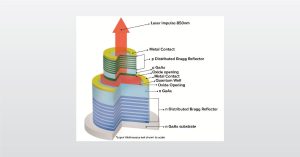
In the full webinar we will introduce analyzing VCSELs with a focus on secondary ion mass spectrometry (SIMS)
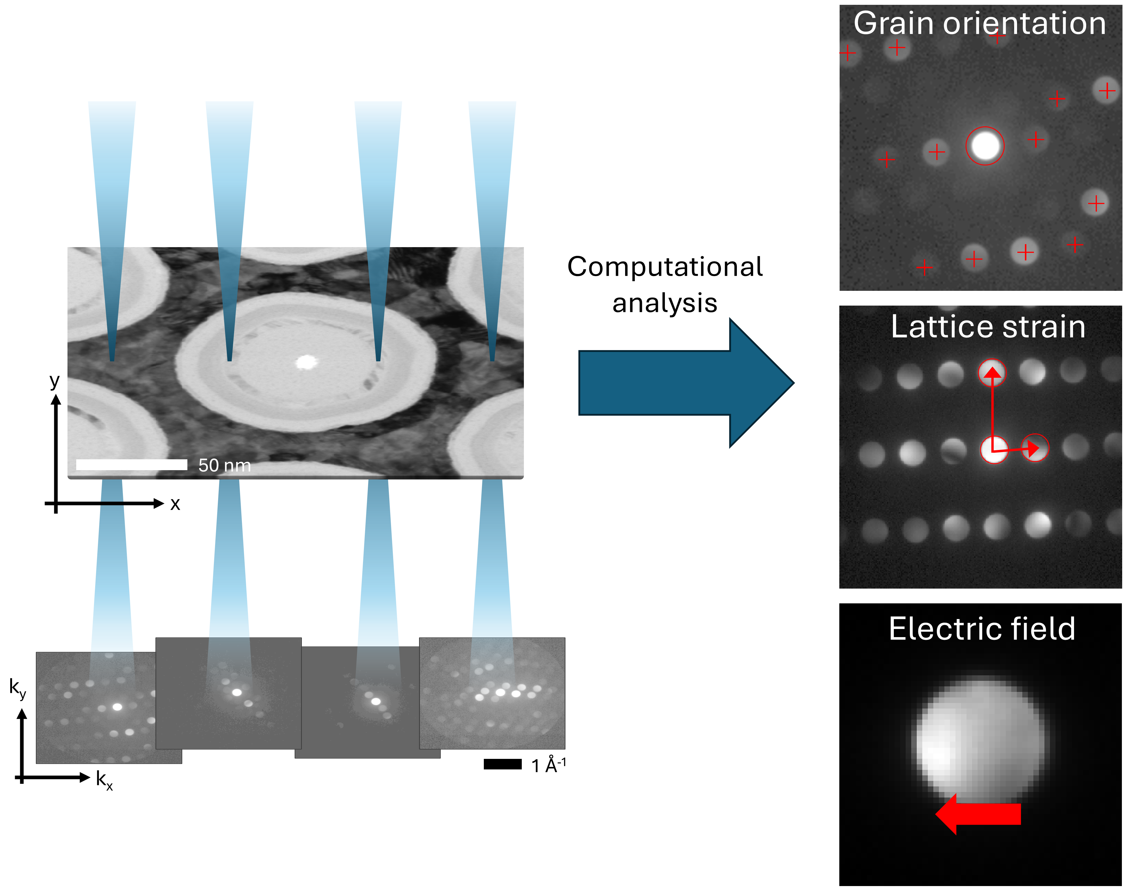
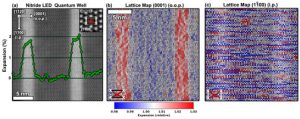
In this application note, we will focus on three applications of 4D-STEM: orientation mapping, strain analysis, and electric field imaging.
June 27, 2024
During this live Ask the Expert event, we will answer pre-submitted questions from our audience regarding Elemental Analysis with Inductively Coupled Plasma (ICP-OES, ICP-MS, LA-ICP-MS). These techniques provide full survey major, minor, trace element analysis, and purity certification for up to 69 measurable elements.
February 12, 2025
During this live Ask the Expert event, we will answer pre-submitted questions from our audience regarding Silicon Carbide for High Powered Electronics. EAG Laboratories has a vast depth of experience analyzing silicon carbide using both bulk and spatially resolved analytic techniques and is the world-leading materials characterization and engineering resource for semiconductor testing.
During this live Ask the Expert event, we will answer pre-submitted questions from our audience regarding materials analysis with various surface contact and optical analytical techniques.
Demand for compound semiconductors has rapidly grown recently. During this live event we answered questions surrounding the Materials Characterization of GaN HEMT power transistors.
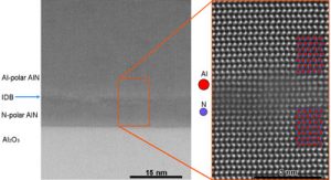
In this application note, we show how different signals obtained through AC-STEM can provide direct observation of local polarity switching.
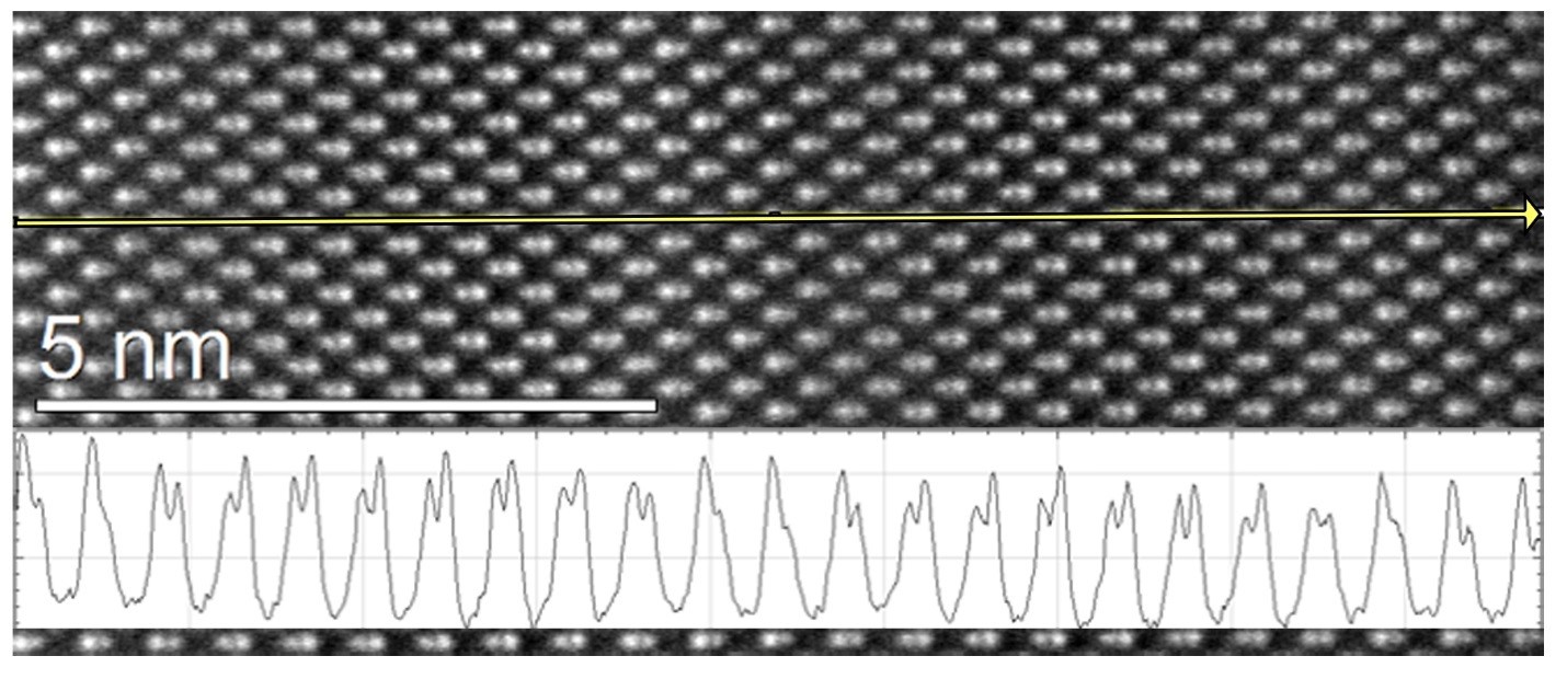
In this application note, we show the possibility to extract distance information at an atom-column to atom-column basis with picometer level precision.
Advances in thin film growth has created a need for characterizing structure and chemistry at the atomic scale using EDS.
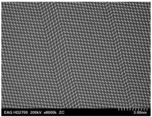
AC-STEM with Secondary Electron (SE) imaging provides the unique capability of evaluating specimen surface morphology with atomic-resolution.

SEM-Cathodoluminescence is used for a wide variety of luminescent materials and devices. It allows for the inspection of optical properties with sub-um spatial resolutions combined with SEM imaging having 3-5nm spatial resolution.
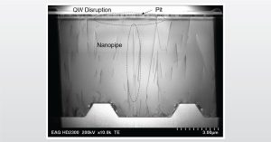
In the full webinar we introduce Characterization and Failure Analysis of Optoelectronic Materials and Devices
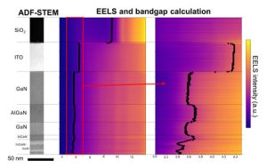
July 29, 2024
Eurofins EAG Laboratories will be presenting Automated Bandgap Measurements in Optoelectronic Devices by Monochromated Electron Energy-Loss Spectroscopy at Microscopy & Microanalysis on July 29th.
Fine control over structural and compositional uniformity during epitaxial growth of compound semiconductors is critical for developing reliable and efficient devices.
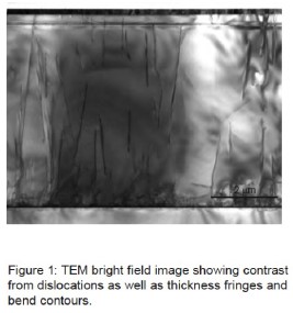
Threading dislocation evaluation of dislocation type in GaN using STEM (AN463) by EAG Laboratories supports LED development and quality.

III-V materials partially provide us with the ever evolving and changing technological advances we enjoy today.
Measurement of dopant & impurity concentrations in compound semiconductors by SIMS with low detection limits & excellent depth resolution.
HR-XRD Measurement of Compound Semiconductors can be used to determine the composition of strained layers and thickness.
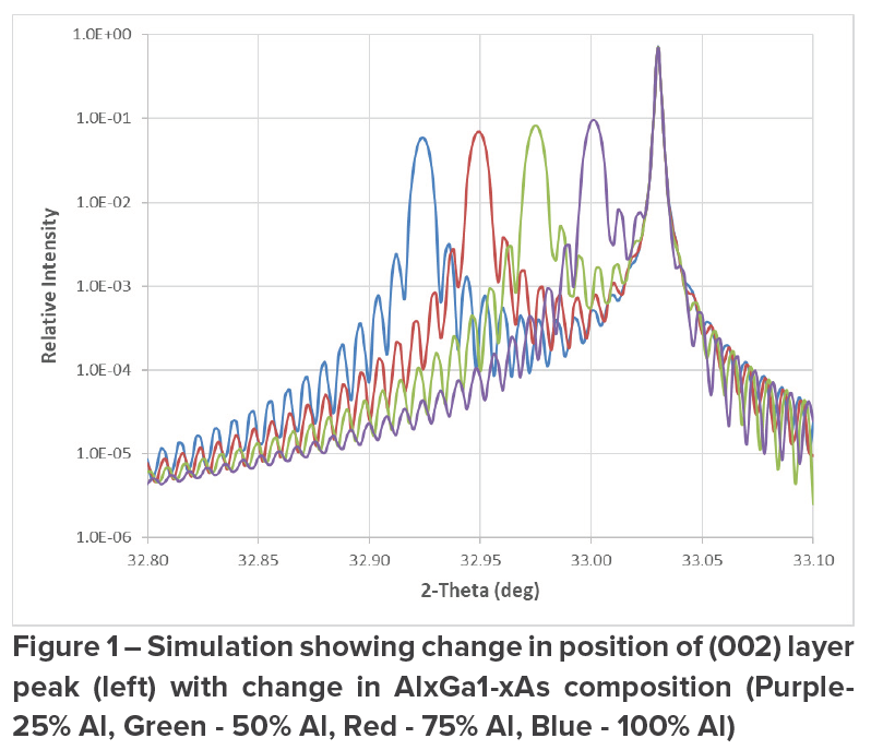
How to determine the composition of epitaxial thin films by X-ray diffraction and will focus on the analysis of AlxGa1-xAs thin films.
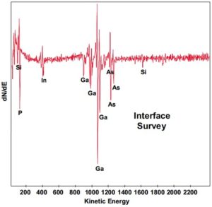
Auger Identification Interface Contamination is discussed regarding the elimination of contaminants for successful semiconductors.
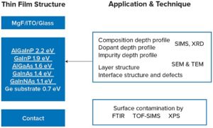
III-V solar cell technology for concentrator PV systems is the focus of this app note, illustrating the way that surface analysis can help

LED characterization, from process control to failure analysis to construction analysis, EAG Laboratories supports your LED analysis needs.

EAG’s material and microelectronic testing service is dedicated to providing the best information from ensuring the purity of starting materials, to prototype testing of devices in the ramp up towards full-scale production.
In the full webinar we introduce MicroLED Analysis for improved understanding of III-nitride material properties and growth/device processes

EAG divides FA tasks into three levels. In each level, we employ optimal techniques for device characterization, defect localization, and root cause failure analysis.
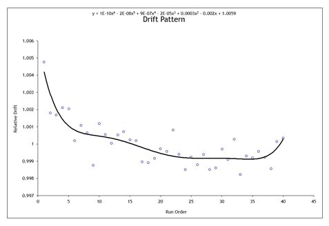
Complex oxides in energy storage, catalysis, sensor/actuation, optics, epitaxy substrates, electronics, bioceramics, structural ceramics

pHEMT device analysis by SIMS improves device performance and aids in failure analysis of III-V high-speed transistor structures.
Point-by-Point Corrected SIMS (PCOR-SIMS) can determine accurate concentrations of matrix elements and dopants in GaN HEMTs.

Measure layer thickness, composition, and doping profiles more accurately than regular SIMS analysis.
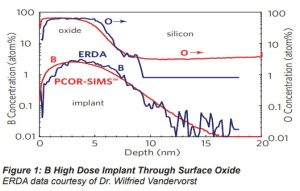
PCOR-SIMS is an EAG proprietary technique that can measure layer thickness, composition, and doping profiles.
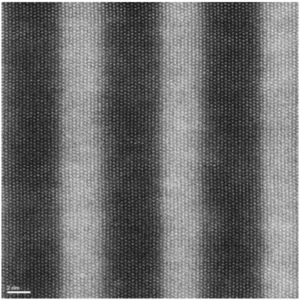
AC-STEM-EDS analysis is explored showing the effectiveness of this technique for characterizing ultrathin layers.
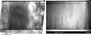
STEM provides images of dislocations with simplified contrast, allowing rapid dislocation typing in both cross section and plan view samples.
When information is required from a compound seminconductor, EAG can depackage and deprocess the sample, & fully characterize it.
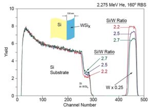
View typical RBS services results from EAG used for compositional thin film analysis for semiconductors, optimal coatings and more.
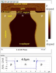
SCM provides doped region distribution mapping, profiling and dimensional analysis for the research and development, failure analysis and quality control of electronic components.
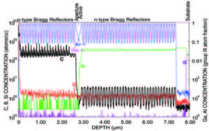
An advanced form of SIMS, PCOR-SIMS identifies dopants, impurities, compositions and thicknesses in various layers of VCSELs
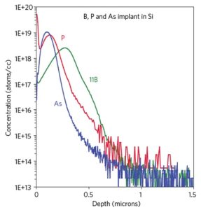
SIMS services from EAG is featured in this technique note, including sample data, showing how SIMS detects low concentrations of impurities
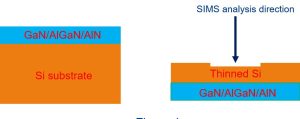
SIMS detects very low concentrations of dopants and impurities. It has been used to study the diffusion of Al and Ga.
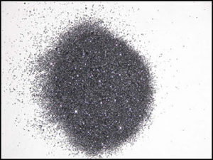
EAG’s SIMS Analysis Individual SiC Particles using a special sample preparation technique eliminates contributions from surface contamination
Raster change technique is used for SIMS measurement of very low levels of nitrogen in Silicon carbide by EAG Laboratories.

Compound semiconductors are responsible for the explosive growth of high-speed electronics, especially in communication applications and advanced mobile appliances.
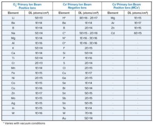
SIMS Detection Limits OF Selected Elements in GaAs, with detection levels are for normal depth profiling conditions of blanket wafers.
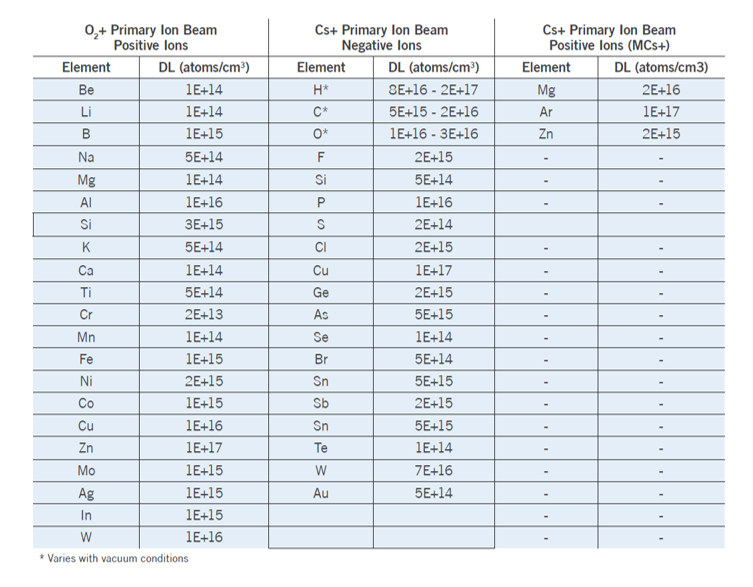
SIMS Detection Limits of Selected Elements in GaN. Normal depth profiling conditions, blanket wafers. Detection levels depends on area.
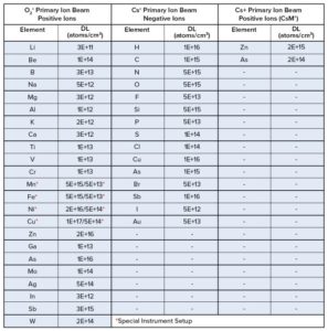
SIMS analytical technique typical detection limits for impurities in a HgCdTe matrix for normal depth profiling conditions.
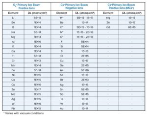
SIMS Detection Limits of Selected Elements in InP for impurities in InP matrices with normal depth profiling conditions.
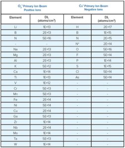
SIMS detection of all elements from H to U with excellent sensitivity. The table provides detection limits for impurities in a SiC matrix.
Silicon Carbide SIMS Measurements provide valuable data for process control and problem solving in wafer growth and device manufacturing.
Contamination control and defect reduction are critical issues in the manufacturing process of compound semiconductor devices which can impact the performance of the end product. We can provide valuable insights to identify contaminants and characterize materials throughout the product lifecycle.

In this webinar we will introduce the principles of Transmission Electron Microscopy (TEM) with a focus on real-world problem-solving.

PCOR-SIMS was originally developed to analyze Silicon Germanium (SiGe) devices for the communications industry.

VCSELs have several advantages, such as a higher modulation speed, which make them great for technological innovations.

Transmission Electron Microscopy is often used to evaluate defects in crystals, but not all defects can be observed with TEM
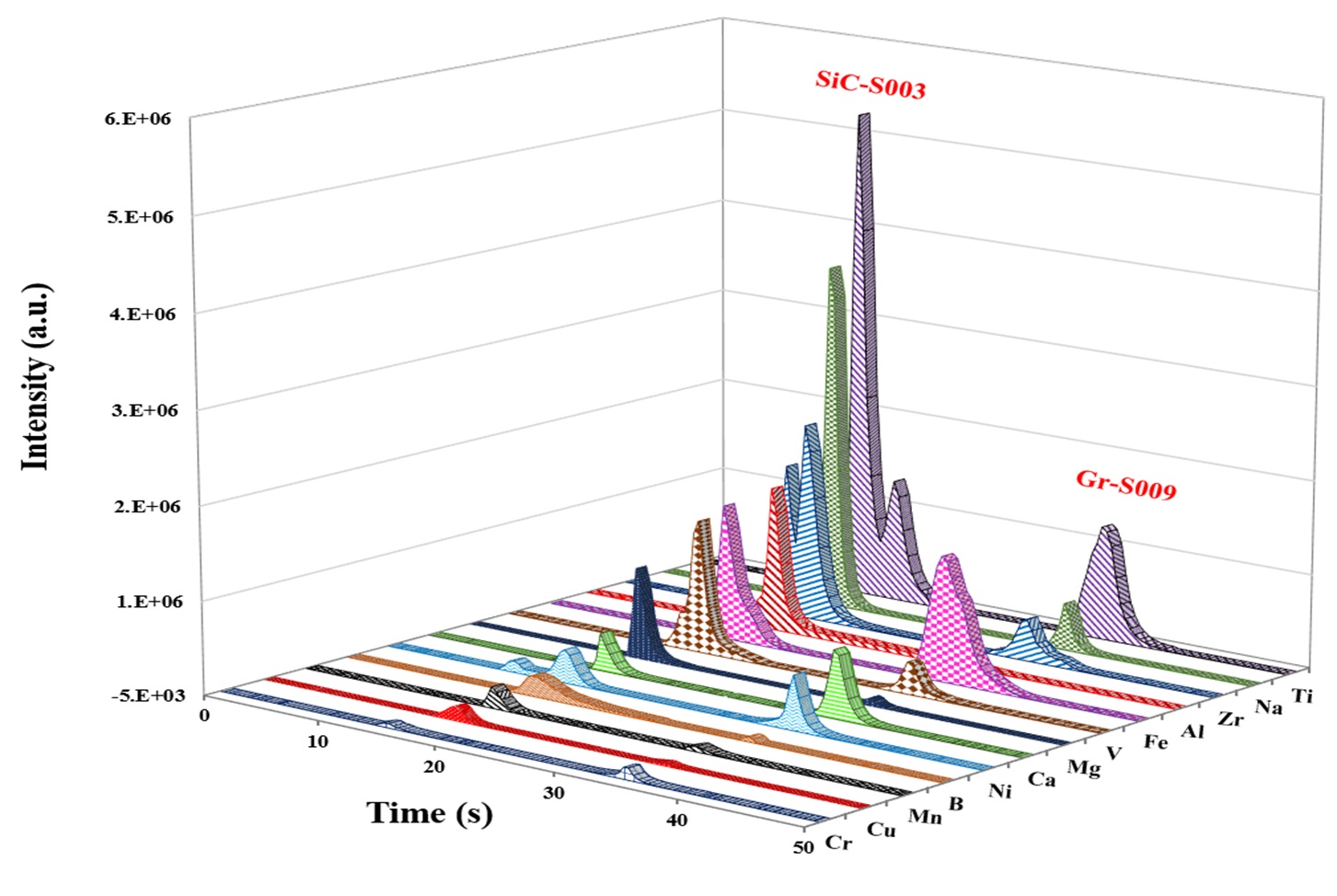
Electrothermal vaporization (ETV) coupled with ICP-OES is an exceptionally sensitive solid sampling technique for purity verifications.
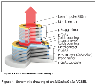
EAG Laboratories to provide comprehensive process development and failure analysis of vertical cavity surface emitting lasers.

AC-STEM analysis can provide a visual representation of non-uniformities in an active region. Roughness can easily be observed within interfaces. EDS maps can then be used to corroborate the roughness in relation to composition.
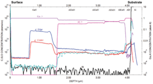
HEMTs characterization using SIMS helps to uncover troublesome impurities, optimize epitaxial layer growth and aid failure analysis
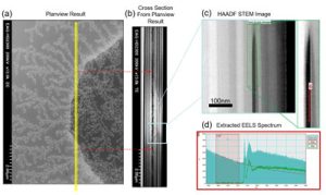
Improper aperture oxidation can lead to high stress or introduce unintended defects ultimately resulting in failure. Here, we present a study using STEM EELS to provide a method for measuring differences in oxygen bonding.
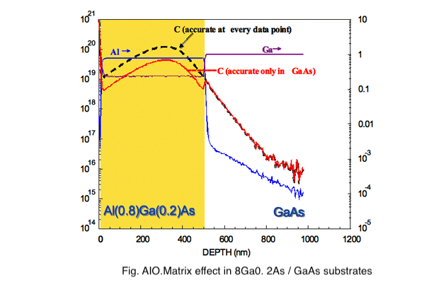
Compound semiconductor films are grown with different matrix compositions that affect the elemental sensitivities and sputtering rates
To enable certain features and improve your experience with us, this site stores cookies on your computer. Please click Continue to provide your authorization and permanently remove this message.
To find out more, please see our privacy policy.