Advanced Materials and Processes Pose Tough Challenges for Electronic Systems Failure Analysis
Home » Advanced Materials and Processes Pose Tough Challenges for Electronic Systems Failure Analysis
As today’s electronics systems continue to shrink in size and become more complex and pervasive, failures can cause costly downtime, product delays and recalls, and debilitating reputational damage. It is important to find and fix failures before they can do damage, but this becomes increasingly challenging when devices are built using advanced materials and processes. The solution is to employ a comprehensive, multi-disciplinary approach to electronic systems failure analysis.
Additionally, many failures can be avoided, altogether, by thorough testing, coupled with the use of the latest focused ion beam (FIB) circuit edit techniques to quickly and inexpensively debug and validate design fixes or explore design optimization opportunities in ICs without having to commit to costly and time-consuming full mask spins.
SYSTEM COMPLEXITY CONTINUES TO GROW AND EVOLVE
Systems are becoming more complex at all levels — board, die, IC and package. Today’s devices can contain billions of transistors, and integrate a wide variety of previously discrete components and independent systems. With the arrival of FinFET, metal gate, low-k dialetric and other advanced process nodes, devices are getting ever smaller. Packaging complexity is also growing, with options including SIP, MCM, SiSub, stacked die, TSV and Cu wire. Additionally, today’s devices increasingly feature multi-layer metal stacks and are produced in flip chip and other advanced chip scale form factors. Meanwhile, the materials, coatings and molding compounds associated with advanced packages and boards are also growing more complex. In the power arena, many devices are moving to silicon carbide (SiC), gallium nitride (GaN) and other wide bandgap materials that create additional challenges related to design and characterization, process monitoring and reliability.
To make the failure analysis problem even more difficult, many failures occur only intermittently. System challenges vary widely by industry and application, with each functional element in a design often requiring specialized domain knowledge in order to understand a failure’s root causes and mechanisms. Networking and automotive systems offer good examples of the breadth and depth of today’s failure analysis challenges. A networking system can span multiple boards containing thousands of components, including complex ICs and SoCs that each might also contain many types of RF, power supply, high-speed digital and storage media. Today’s automobiles are similarly complex, containing as many as 100 electronic control units (ECUs), or more, for systems ranging from backup cameras to lane-changing warning systems, and tomorrow’s assisted-driving and sensor-guided autopilot systems are expected to include a dozen ultrasonic detectors and multiple cameras and radar sensors. Failures can occur anywhere in a complex chain of stand-alone and multiple interrelated systems. Meanwhile, counterfeit components may also have entered the automotive supply chain, introducing additional risks and accentuating the need for screening and analysis plus various types of verification and authentication tests against reliability specifications.
FAILURE ANALYSIS: THE FIRST LINE OF DEFENSE
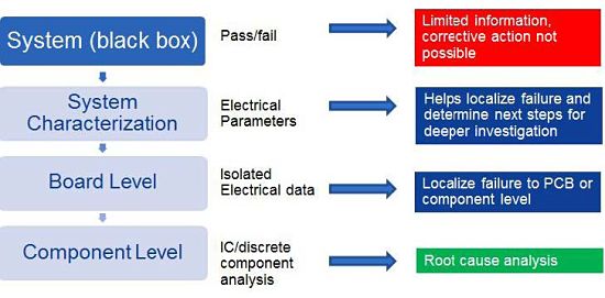
The ideal failure analysis approach must span both electrical and physical analysis to optimize root cause identification and determine the associated failure mechanism and how to prevent future failures. The focus must be on the entire system, including the electronics, materials, and failure mechanisms occurring at the IC transistor level (see Fig. 1).
The ideal failure analysis approach must span both electrical and physical analysis to optimize root cause identification and determine the associated failure mechanism and how to prevent future failures. The focus must be on the entire system, including the electronics, materials, and failure mechanisms occurring at the IC transistor level (see Fig. 1).
Effective failure analysis also requires highly experienced and well-trained engineers and technicians with expertise that extends from the component to the system level, and they must have at their disposal a comprehensive set of lab equipment. Failure analysis service providers also must be able to perform parallel processing of large projects, and they should have the capability to scale their services as client needs dictate. Other key ingredients include system redundancy and such specialized equipment as advanced high-resolution microscopy imaging systems that enable component-level analysis. To handle failure characterization, labs also must have such fundamental capabilities as x-ray, thermal mapping, curve trace, time domain reflectometry, and functional test equipment, as well as more advanced tools such as laser timing probe for real-time, no-loading, non-contact signal waveform acquisition. At advanced nodes below 28nm, nano-probing and more sophisticated equipment may also be necessary, so that failures can be localized down to a single transistor, if necessary.
Sometimes, materials analysis using various spectroscopy techniques (EDS, Raman) or X-ray (diffraction, reflectivity, or flouorescence) can also be useful to characterize materials issues.
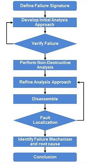
Also critical is a comprehensive methodology and work flow (see Fig. 2), beginning with a definition of the electrical failure signature, and continuing through failure mechanism identification and problem resolution. In order to address multiple complex and interdependent components and features, the process must also include disciplined and periodic refining of the analysis approach based on data and incremental findings. This approach typically involves developing hypotheses and then working to validate or reject them. Various experiments may also be necessary, in order to duplicate and/or model a given failure.
It is often critical to customization the failure analysis approach, as well. Each situation has its own specific characteristics and issues to address, eliminating the possibility of a “one size fits all” approach. Each situation requires a methodical approach that begins the right questions so that a customized workflow can be developed.
PREVENTING IC FAILURES BEFORE THEY OCCUR, WITH THOROUGH TESTING AND USE OF FIB CIRCUIT EDIT
Another strategy for decreasing failures is to employ thorough testing of ICs and follow-up use of FIB circuit edit during the development process, especially at advanced process nodes where it would be difficult, if not impossible, to anticipate future problems based on previous design work. Electrical characterization, functional testing, and reliability qualification can help uncover many issues before products are released to production. Once issues are identified, FIB circuit edit can be used during the process of debugging and validating fixes to in-progress designs, or exploring design optimization changes before committing to the high cost and lengthy timetables of a full mask spin.
Barriers to success can be even higher at advanced process nodes because of high mask costs and greater difficulty associated with finding and fixing bugs. It can be extremely difficult to anticipate problems at these nodes based on experience gained during earlier design work. Devices manufactured at today’s 20-nm process nodes have 10 times smaller feature sizes than the laser light wavelength that is generally used in lithography. At these advanced nodes, pre-silicon testing is more difficult, simulations take much longer, and it is impossible to fully verify many designs. Even more problematic are extremely complex designs that may have flawed simulation models, and which can easily be stressed by their packaging.
With each new technology node, design and integration complexity grows. Challenges range from multiple patterning and layout-dependent effects (LDE) to the use of local interconnect layers. Server signals and power electro-migration can also create difficulties. The smaller the metal pitch becomes, the more chance of coupling effects and signal integrity issues. Higher wire and via resistance also requires more advanced and variable wire sizing and tapering techniques. There are also challenges related to extraction, timing, signal integrity analysis, and modeling, and each must account for many variation issues in order to ensure accuracy without jeopardizing performance. Plus, lithography limitations at 20 nm often create the need for significant fixing in order to achieve signoff. Finally, there are many different chip and intellectual property (IP) integration challenges, packaging issues, and additional complexity as all of these issues interact with one another.
To address some of these issues, EDA tool providers are already offering advice related to design flow and other solutions to difficult technical challenges. Beyond these design flow modifications, however, developers can also apply FIB circuit edit at the prototype stage during debug. The same techniques can also be employed to explore design optimization opportunities, enabling developers to quickly and inexpensively create, test and validate physical prototypes before committing to the high cost or lengthy timetables of a full mask spin.
FIB-edited device prototypes can then be used on a one-time basis to guide mask modifications, as an alternative to successive trial-and-error mask versions.
With today’s solutions, it is possible to edit circuits fabricated with 28 nm and smaller technology nodes that feature multiple-layer metal stacks and occupy flip chip and other advanced chip scale form factors.
To perform the edits, a nanoscale-resolution, gallium (Ga+) ion beam is used in the process of imaging, etching and depositing materials on the IC. This is done with an extremely high level of precision. To cut and connect circuitry within the live device, material is removed and deposited, and the same process can also be employed to create probe points that are used for electrical test (see Fig 3).
Advances in tools, methodologies and techniques have improved beam guidance, enabling operators to perform more intricate operations, in smaller areas, on both the back and front sides of the device, and to handle copper layers.
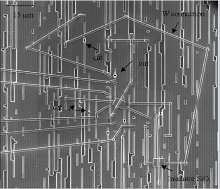

To locate areas of interest, the FIB tool is coupled to a CAD navigation system and the designer’s GDS files are typically used to navigate to the precise area. This provides a very precise method for finding subsurface features and ensuring that the right edits are made (see Fig. 4). One of the most important requirements for successful FIB circuit edit is the ability to accurately position the beam.
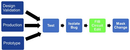
There are a variety of valuable applications for FIB circuit edit at every commercial available node, including verifying design change on the tester and validating that change at the system board level. The process can be implemented both at the simulation stage and later during de-bug to optimize success rates during the IC design process (see Fig. 3). Typical applications include debugging and optimizing devices in production, exploring and validating design changes, and prototyping new devices without costly and time-consuming mask set fabrication.
FIB circuit edit also can be used to scale fixes to a handful or tens of devices to provide samples to internal test, validation and qualification teams and even customers.
Finally, FIB circuit edit can be used to accelerate time-to-market, speeding up the entire cycle for getting customers into production and avoiding loss of reputation or late penalties, or keeping potential competitors from getting their foot in the door.
Electronic system failures are becoming increasingly difficult and expensive to identify, diagnose and resolve. The stakes have never been higher to quickly find and fix them before they create problems. This requires a comprehensive, multidisciplinary electronic system failure analysis methodology and workflow that extends from the component to system level and is backed by specialized expertise and equipment. Meanwhile, the challenges associated with IC design verification and validation continue to intensify as nanoscale geometries move downward.
Adding FIB circuit edit to an overall failure analysis and resolution arsenal can significantly increase design success rates and preempt failures before they happen, by improving debug and validation, and making it easier to explore design optimization opportunities without committing to a full mask spin.
Would you like to learn more about Electronic Systems Failure Analysis?
Contact us today for your electronic system failure analysis needs. Please complete the form below to have an EAG expert contact you