Auger Electron Spectroscopy (AES) Tutorial
Home » Auger Electron Spectroscopy (AES) Tutorial
In this Auger Tutorial from EAG Laboratories, we present the history of Auger, as well as the scientific principles behind the instrumentation, theory and data provided by this analytical technique.
History
In 1923, Pierre Auger discovered the Auger Process and Auger electrons while irradiating samples with X-rays. The idea of using electron-stimulated Auger signals for surface analysis was first suggested in 1953 by J. J. Lander. However, it wasn’t until 1967 that Larry Harris demonstrated the use of differentiation for enhancing the Auger signals. This development provided the necessary sensitivity for useful measurements. Early differentiating instruments used analog circuits and lock-in amplifiers to provide differentiated spectra directly, but more modern instruments acquire electron intensities directly and use computer Display Algorithms to provide differentiated spectra. Today Auger electron spectroscopy is the most frequent analytical method for surfaces, thin-films, and interface compositions. This utility arises from the combination of surface specificity (0.5 to 10 nm), good lateral surface resolution (as little as 10 nm), periodic table coverage (except hydrogen and helium), and reasonable sensitivity (100 ppm for most elements).
Electron Energy Analyzers
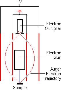
Electron energy analyzers measure the number of ejected electrons as a function of the electron energies. The analyzers must be located in a high vacuum chamber and isolated from stray magnetic fields (including the earthís) that deflect electrons. Past Auger spectrometers used several types of electron energy analyzers, including spherical sector and cylindrical mirror analyzers. However, modern instruments nearly always incorporate cylindrical mirror analyzers because their high transmission efficiency leads to better signal-to-noise ratios. The schematic shows a cross section of a cylindrical mirror analyzer in red. The primary electron beam hits the sample surface at the source point of the analyzer. Auger electrons move outward in all directions and some pass through the grid covered aperture in the inner cylinder. A variable negative potential on the outer cylinder bends the Auger electrons back through a second aperture on the inner cylinder and then through an exit aperture on the analyzer axis. The energy of transmitted electrons is proportional to the voltage (-V) on the outer cylinder.
Primary Electron Sources
Three kinds of primary electron sources are in common use in Auger electron spectrometers.
- A tungsten cathode source consists of a wire filament bent in the shape of a hairpin. The filament operates at ~2700 K by resistive heating. The tungsten cathodes are widely used because they are both reliable and inexpensive. Lateral resolution is limited because the tungsten cathode current densities are only about 1.75 A/cm2.
- Lanthanum hexaboride (LaB6) cathodes provide higher current densities because LaB6 has a lower work function and greater emissivity than tungsten. At 2000 K, current densities of ~100 A/cm2 are available. Higher current densities provide narrower electron beams useful for analyzing smaller features.
- Field Emission electron sources consist of very sharp tungsten points at which electrical fields can be >10E7 V/cm. At these fields, electrons tunnel directly through the barrier and leave the emitter with near zero work functions. Field emission guns provide the brightest beams (1E3 to 1E6 A/cm2). However, the low work functions are only obtained with extremely clean tips. A single atom on the tip can increase the work function and reduce electron emission. Ultrahigh vacuum and continuous heating (~2000 K) keep the tip clean and the electron beam stable. Electron beams as narrow as 10 nm provide Auger analysis of small features.
Auger instruments have primary electron beam columns similar to electron microscopes. The columns may include both electrostatic and magnetic lenses for beam focusing as well as quadrupole deflectors for beam steering and octopole lenses for beam shaping.
Detectors
Auger electron spectrometers use electron multipliers similar to those used in SIMS. The Auger electron multipliers usually operate in pulse counting mode which records every electron as it arrives at the detector.
Auger instruments have primary electron beam columns similar to electron microscopes. The columns may include both electrostatic and magnetic lenses for beam focusing as well as quadrupole deflectors for beam steering and octopole lenses for beam shaping.
Modern Auger Instruments
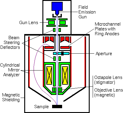
One modern Auger electron spectrometer incorporates both a field emission electron source and a parallel electron detector. The parallel detector simultaneously records electrons at eight separate energies. The detector consists of a dual microchannel plate with a hole in the middle to accommodate the primary beam. Eight concentric ring anodes detect electrons arriving with eight separate energies.
Auger Data Display Algorithms
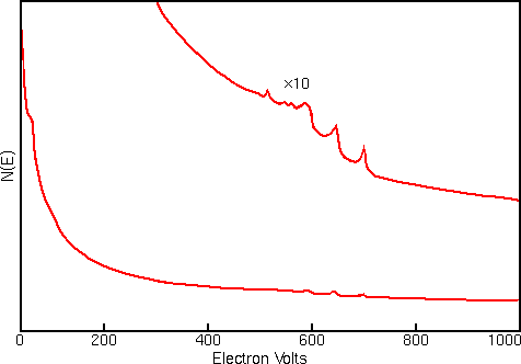
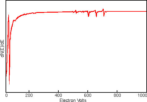
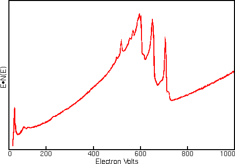
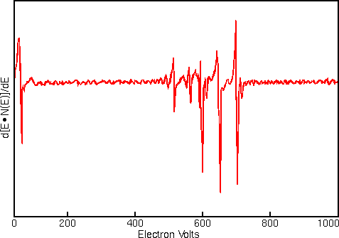
Displaying Auger spectra as differentials enhances the sharp Auger peaks and deemphasizes the relatively intense and structureless background. Strong interfering signals accompany the Auger electrons in all regions of the Auger spectrum. The interference includes contributions from secondary and backscattered electrons, and from Auger electrons that have lost energy as they escape from beneath the sample surface. The first figure shows a typical Auger spectrum (of iron) plotted as total electron signal, N(E), versus electron energy. The Auger peaks are obscure even after expanding the vertical scale.
Related Techniques
Three other analytical techniques use some of the same key instrument components as Auger electron spectrometers. Scanning electron microscopy and electron probe microanalysis both employ focused electron beams to excite the sample and X-ray photoelectron spectroscopy employs an electron energy spectometer to measure energies of emitted electrons.
Scanning Electron Microscopy
Scanning electron microscopy (SEM) instruments and Auger spectrometers use similar primary electron columns. In fact,SEM capabilities are usually incorporated into Auger instruments. Separate detectors are required for secondary and backscattered electrons. To produce images, these electron signals are measured as a function of primary beam position while the beam is scanned in a raster pattern over the sample.
The scintillator-photomultiplier electron detector (called an Everhart-Thornley detector, after its inventors) measures the secondary electrons. Higher voltages on the Faraday cage draw in more secondary electrons with more diverse trajectories. Off-axis detector placement favors secondary electrons with trajectories leading toward the detector. This provides the topographical information characteristic of secondary electron images.
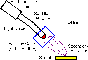
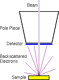
The backscattered electrons are usually measured with a solid state detector located on the primary beam pole piece. The detector consists of a diode with a thin gold conductor across the front surface. Backscattered (but not secondary) electrons have sufficient energy to pass through the front surface and produce electron hole pairs which produce a current in the diode.
The secondary and backscattered electron signals are much more intense than the Auger signals. Therefore, Auger electron measurements require more intense primary beams to provide sufficient Auger electron signals. Auger instruments provide higher primary beam intensities and accept larger beam diameters as a trade-off. This maximizes the Auger electron signals at the expense of lateral resolution. Since the secondary and backscattered signals are more intense, a primary column dedicated only to SEM can be optimized for lateral resolution.
Nevertheless, modern Auger instruments provide reasonably high resolution (< 10 nm) SEM images. Most stand-alone Auger instruments come equipped with both secondary and backscatter detectors.
For a thorough discussion of scanning electron microscopy (and electron probe X-ray microanalysis) see J. I. Goldstein, D. E. Newbury, P. Echlin, D. C. Joy, C. Fiori, and E. Lifshin, Scanning Electron Microscopy and X-Ray Microanalysis, Plenum Press, New York, 1981, and D. E. Newbury, D. C. Joy, P. Echlin, C. E. Fiori, and J. I. Goldstein, Advanced Scanning Electron Microscopy and X-Ray Microanalysis, Plenum Press, New York, 1986.
Electron Probe X-Ray Microanalysis
The sample is bombarded with an electron beam in electron probe X-ray microanalysis. The X-rays formed in competition with the Auger process serve as the measurable signal. Two kinds of X-ray detectors are in wide use. Energy dispersive spectrometry (EDS) relies on semiconductor detectors, usually lithium drifted silicon. The EDS detector converts the X-rays into electron-hole pairs by inelastic scattering. The principle of operation is similar to the surface barrier detectors used in RBS. Wavelength dispersive spectrometry (WDS) depends on Bragg diffraction of X-rays incident on a crystal. Any X-ray wavelength can be selected by adjusting the crystal angle and/or changing the crystal to provide different diffraction plane spacing. The two detectors are complementary.
The EDS system detects all X-ray energies simultaneously and accepts a wide solid angle of the X-ray emission. Thus, EDS is faster and better for survey spectra when the sample is totally unknown. The WDS system provides higher energy resolution, useful for separating overlapping peaks. Furthermore, bremsstrahlung contributes less background to the narrower peaks. In addition, WDS detectors accept a wider range of signal intensities. The WDS system is useful for mapping the locations of specific elements over a sample surface and for elemental quantitation down to the 100 ppm level.
X-Ray Photoelectron Spectroscopy
X-Ray photoelectron spectroscopy (XPS) measures the energy distribution of photoelectrons produced by sample irradiation with X-rays. The photoelectron energies follow the Einstein photoelectric law (kinetic energy = photon energy – binding energy). The Auger process also contributes peaks to XPS spectra. The theory and instrumentation of XPS are described in another section.
Auger Electron Spectroscopy (AES) Theory
Auger electron spectroscopy (AES) identifies elemental compositions of surfaces by measuring the energies of Auger electrons. Auger electron emission is stimulated by bombarding the sample with an electron beam. The Auger electron energies are characteristic of the elements from which the electrons come. Auger electron spectroscopy is a widespread method for analysis of surfaces, thin films, and interfaces.
Although both are dated, two good reference book are:
- Photoelectron and Auger Spectroscopy, T. A. Carlson (Plenum Press, New York, 1975)
- Methods of Surface Analysis, A. W. Czanderna, ed. (Elsevier, New York, 1975)
The Auger Process
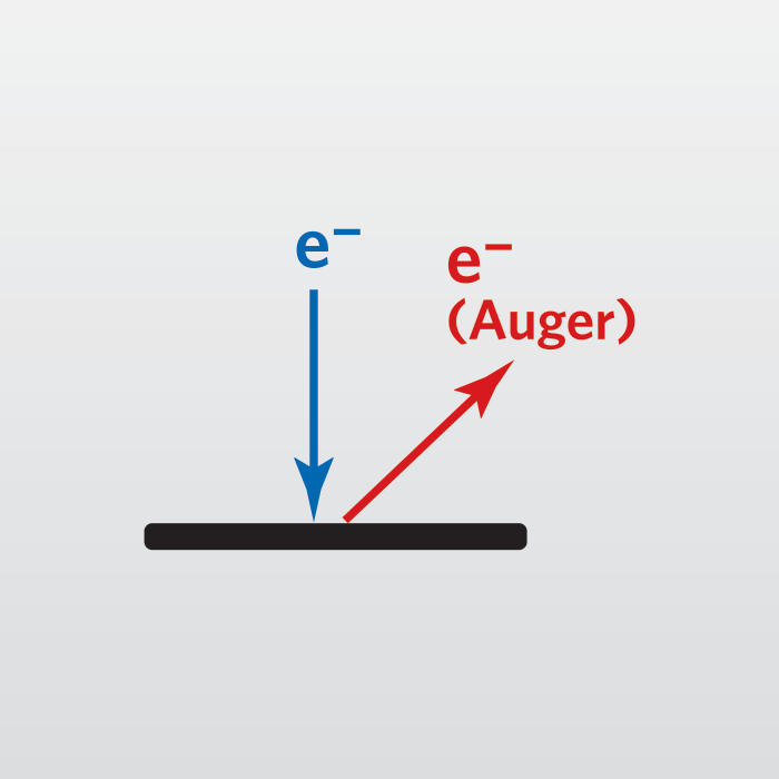
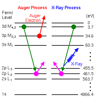
The basic Auger process starts with removal of an inner shell atomic electron to form a vacancy. Several processes are capable of producing the vacancy, but bombardment with an electron beam is the most common. The inner shell vacancy is filled by a second atomic electron from a higher shell. Energy must be simultaneously released. A third electron, the Auger electron, escapes carrying the excess energy in a radiationless process.
The process of an excited ion decaying into a doubly charged ion by ejection of an electron is called the Auger process. Alternatively, an X-ray photon removes the energy. For low atomic number elements, the most probable transitions occur when a K-level electron is ejected by the primary beam, an L-level electron drops into the vacancy, and another L-level electron is ejected. Higher atomic number elements have LMM and MNN transitions that are more probable than KLL.
The figure illustrates two competing paths for energy dissipation with titanium as an example. The illustrated LMM Auger electron energy is ~423 eV (EAuger = EL2 – EM4 – EM3) and the X-ray photon energy is ~457.8 eV (Ehv = EL2 – EM4).
Electron Beam Effects
When the electron beam strikes a sample surface, it produces a plethora of different interactions. Elastic scattering occurs when a high energy electron (1 to 30 keV) strikes a sample atom and recoils with essentially all of its energy. (The RBS kinematic factor equation applies to this situation and indicates an energy loss of 1 eV for a 25 keV electrons striking a surface iron atom and scattering back at 180 degrees.) The electron beam loses energy as it passes through material, thereby broadening the energy distribution of backscattered electrons. Inelastic scattering occurs by several mechanisms as the primary electron gives up larger amounts of its energy.
- Plasmon excitation, occurs with high probablility as the free electron gas between ionic cores absorbs energy. Typical plasmon excitations involve transfer of around 15 eV to the solid.
- Conduction band excitation ejects loosely bound conduction electrons as secondary electrons. The majority leave with 0 to 50 eV kinetic energies.
- Bremsstrahlung (from the German for “braking radiation”) occurs when a primary electron undergoes deceleration in the Coulombic field of an atom. The bremsstralung consists of X-ray photons with energies spread between zero and the primary beam energy.
- Excitation of lattice oscillations (phonons) transfers a substantial portion of beam energy to the sample as heat.
- Inner shell ionization leaves the atom in an a highly energetic state while absorbing a large amount of primary electron energy. Decay of this excited state produces characteristic Auger electrons and X-rays.
Auger Analytical Volumes
Auger Electron Spectroscopy
Auger electron spectroscopy (AES) identifies elemental compositions of surfaces by measuring the energies of Auger electrons. An Auger spectrum plots a function of electron signal intensity versus electron energy. The Auger energies fall between secondary electron energies on the low end and backscattered electron energies on the high end. Those backscattered electrons that recoil with 100 % of their primary energy form the elastic peak.
The terms secondary and backscattered are sometimes defined in the operational terminology of scanning electron microscopy (SEM). The true secondary electrons have energy less than ~50 eV. They can be detected with the SEM secondary electron detector biased at +50 to +200 V. All electrons with too much energy to be trapped in the secondary electron detector fall in the backscattered category.
The Auger electrons start with narrow energy distributions, but they soon lose energy as they pass through materials. Auger electrons fail to emerge with their characteristic energies if they start from deeper than about 1 to 5 nm into the surface. Thus, Auger analysis is surface specific. Auger electrons that escape from deeper in the sample contribute loss tails to the spectrum background. The secondary and backscattered electrons have broad energy distributions that tail into the Auger region. The sum of these interfering signals is much greater than the Auger signals themselves. Auger display algorithms use differentiation to enhance the signal relative to the interferences.
Uses of Auger
Auger electron spectroscopy provides compositional information for many types of surfaces, thin films, and interfaces. Typical samples include both raw semiconductors materials and finished electronic devices. Many of these devices consist of thin layers. For example, Auger can distinguish between Si, SiO2, SiO, and Si3N4 in a 10 nm layer on a silicon wafer.
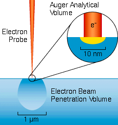
Auger analytical volumes down to about 3e-19 cc are possible. It is common to analyze individual small features within finished or partly finished electronic devices. Many other analyses rely on this microanalytical capability for characterizing heterogeneous materials. For example, Auger analyses of failed materials are common. The fractured surfaces of a broken piece of steel might be examined for the presence of unusual elements such as lead at metal grain boundaries. In contrast to Auger, less finely focused microanalytical techniques provide only average concentrations from larger analytical volumes.
Limitations of Auger
Although widely useful, Auger does have limitations. It cannot detect hydrogen or helium. It does not provide for nondestructive depth profiles. It requires that samples be small and compatible with high vacuum. Nonconducting samples sometimes charge under electron beam bombardment and simply can’t be analyzed. Elemental quantitation by Auger depends on instrumental, chemical, and sample related factors.
Auger Electron Energies
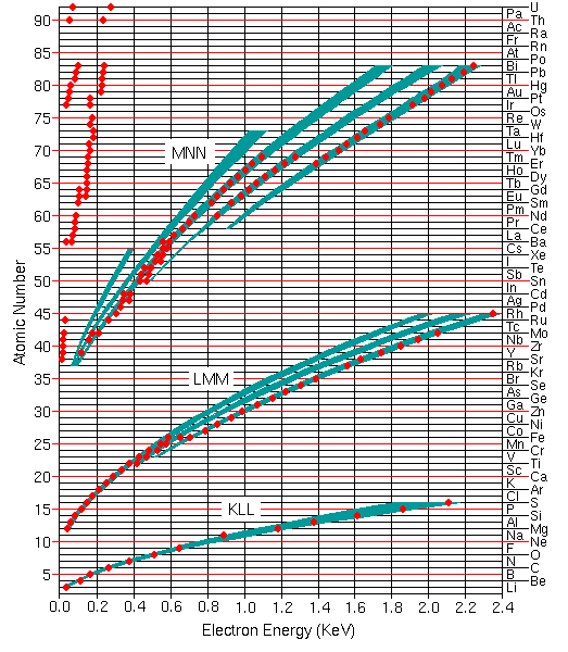
Qualitative analysis by Auger electron spectroscopy depends on identification of the elements responsible for the various peaks in the spectrum. The Auger electron energies are widely tabulated for all elements in the periodic table. The figure shows the most useful Auger peaks in the KLL, LMM, and MNN parts of the spectrum as well as higher transitions for elements above cesium. The red dots indicate the strongest and most characteristic peaks and the green bands indicate the rough structure of less intense peaks.
Elemental Quantitation
Auger electron peaks are proportional to elemental concentrations. However, it is seldom possible to measure concentrations from first principles. Several instrumental factors influence Auger peak heights. These include primary beam energy, sample orientation, and the energy resolution and acceptance angle of the analyzer.
The chemical states of elements in the sample also influence the process of elemental analysis by Auger. Both peak intensity and peak shape vary, especially as a function of oxidation state. Changes in peak shape are important when the quantitation proceeds from a differential data display.
Sample heterogeneity must be considered for quantitative analysis. The sample should be homogeneous in the lateral directions relative to the primary beam diameter for measurements to be accurate. The Auger signals arise from an analytical volume that depends mainly on the diameter of the primary beam. If the beam is narrower than the scale of heterogeneity, then meaningful analyses can be made on islands within a sample. The thickness of the analytical volume is small because Auger is highly surface sensitive. Therefore, the analyzed surface may not be representative of the bulk material. For example, many metal samples acquire thin oxide coatings when exposed to air. In spite of the above considerations, quantification of elemental concentrations is possible in cases where relative sensitivity factors have been measured in the same sample matrix.
A typical Auger analysis requires quantification of major and minor elements. This concentration range is consistent with Auger analytical detection limits (1 to 0.01 %). (In contrast, SIMS usually provides trace element quantification while the major elements remain essentially constant.) Since concentrations of all elements, (including the matrix) can vary in an Auger measurement, it is necessary to express concentrations as percents (CE%) normalized relative to the sum of all others.

The next part of the procedure uses the same logic as SIMS RSFs.
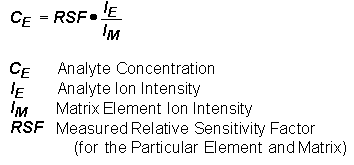
Substituting the right side of the RSF equation for concentrations (CE and CX) in the top equation (and eliminating the matrix current terms from the numerator and denominator) give the following equation. This format is the most common method for elemental quantification by Auger. However, it should be noted that Auger RSFís are often reciprocals of those defined here. (They must be incorporated by division into the Auger signal rather than multiplication.)

Auger Electron Emission Probabilities
The Auger electron is the final electron in the Auger emission process. The primary excitation beam removes the first electron from a core level of an analyte atom to produce a vacancy. A second electron falls from a higher level into the vacancy with release of energy. The resulting energy is carried off with the Auger electron which is ejected from a higher energy level.
Auger Depth Profiling
To analyze samples in depth, Auger instruments incorporate ion beam sputtering to remove material from the sample surface. One cycle of a typical depth profile consists of sputtering a small increment into the sample, stopping, measuring relevant portions of the Auger spectrum, and using the equation for elemental quantification.
Would you like to learn more about Auger Electron Spectroscopy (AES)?
Contact us today for your Auger Electron Spectroscopy (AES) needs. Please complete the form below to have an EAG expert contact you.