LED Analysis
Home » LED Analysis
EAG has a broad range of analytical services developed exclusively for LED characterization. Our analytical staff, in combination with our specialized instrumentation are ready to help with your research & development, process control, failure analysis and construction analysis needs.
CONSTRUCTION ANALYSIS — PACKAGE LEVEL
Identification and measurement of the materials, structure, composition and dopant profiles that comprise an LED.
ENCAPSULANT
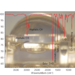
Polymer materials can be evaluated and identified using FTIR (Fourier Transform Infrared Spectroscopy). In this case the material is a modified epoxy.
PACKAGE
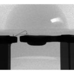
The structural integrity of LED packages and wire connections can be evaluated non-destructively using RTX (Real Time X-ray) analysis.
STRUCTURE
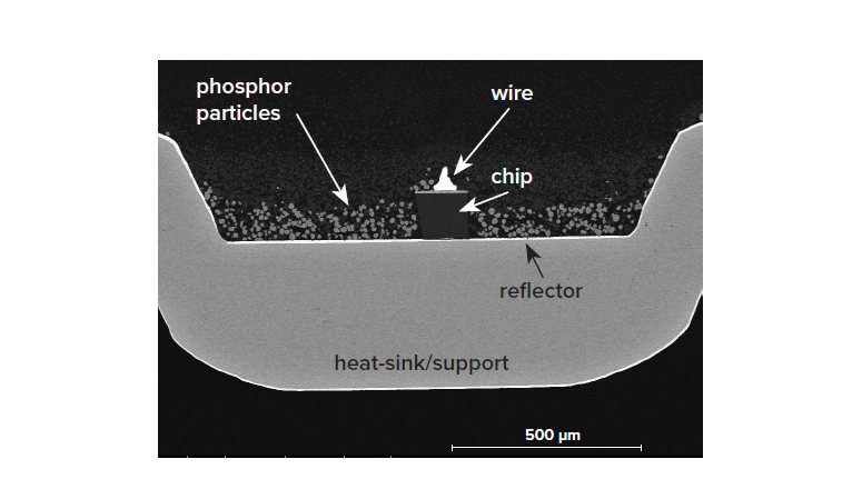
Materials and layout of the package and support structures can be examined in cross- section using SEM (Scanning Electron Microscopy) imaging and EDS (Energy Dispersive X-ray Spectroscopy) analysis.
PHOSPHORS
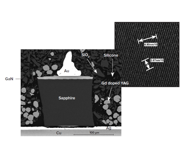
Materials identification in and around the LED chip can include evaluation of the phosphors. In this case STEM (Scanning Transmission Electron Microscopy)/EDS identified the phosphor as Gd doped YAG (Yttrium-Aluminum Garnet). Lattice imaging and d-space measurements confirm YAG.
CONSTRUCTION ANALYSIS — DIE LEVEL
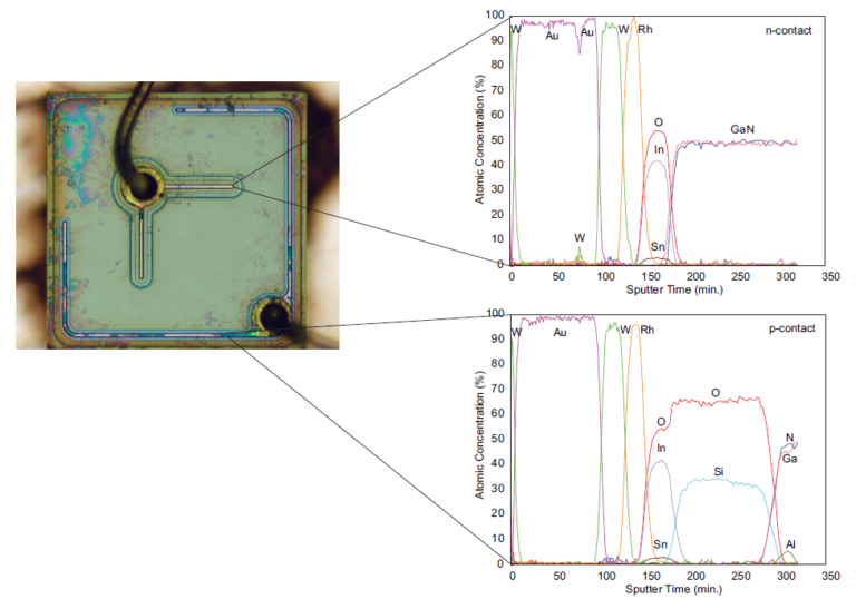
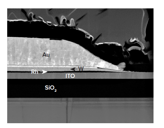
n and p contact evaluation by Auger (Auger Electron Spectroscopy) depth profiling
EPI-LAYER STRUCTURE
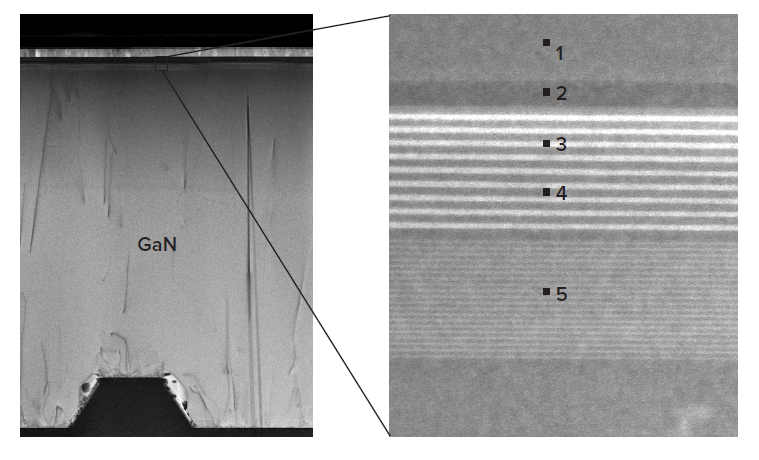
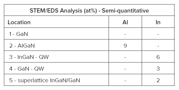
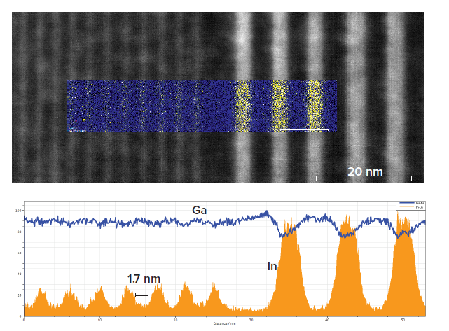
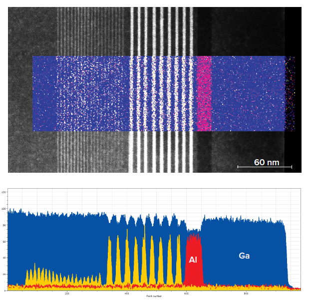
Composition of InGaN and GaN within the QW can be partially resolved by STEM/EDS. Composition within the superlattice layers cannot be resolved.
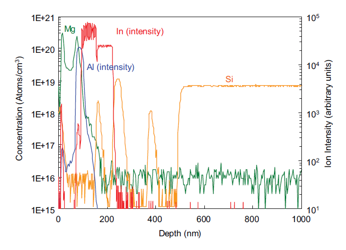
DOPING PROFILE
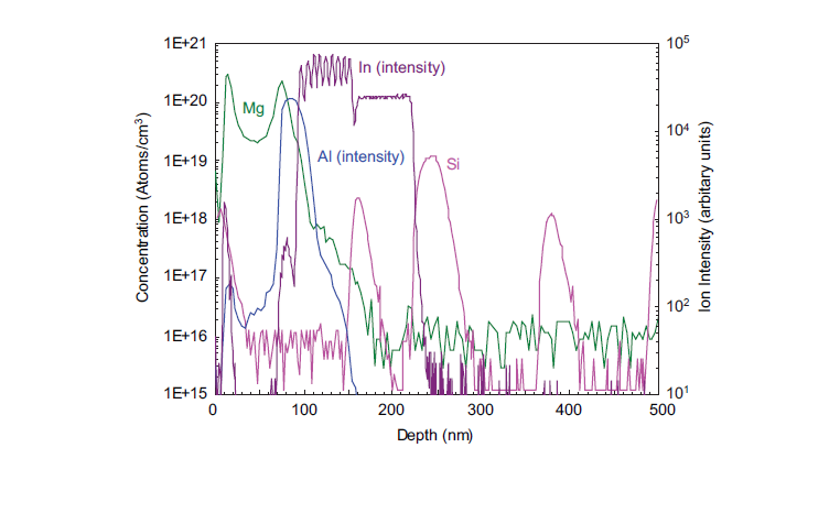
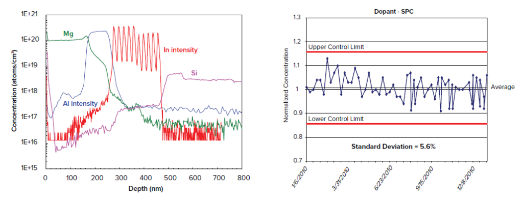
SIMS (Secondary Ion Mass Spectrometry) depth profile analysis for Mg and Si doping profiles in GaN / AlGaN / InGaN epi-layers.
FAILURE ANALYSIS
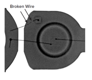
PACKAGE AND WIRE INTEGRITY
RTX examination of LED can reveal open wires.
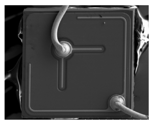
DECAP
LED packaging can be difficult to remove. EAG has developed methods to decapsulate while preserving electrical functionality
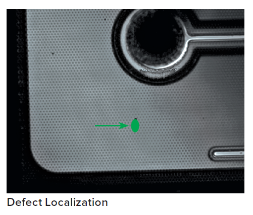
HOT SPOTS
Examination by OBIRCH (Optical Beam Induced Resistance Change) can reveal defect sites.
FAILURE SITE
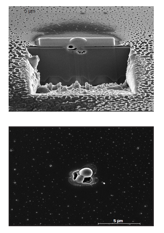
SEM examination of the defect site identified by OBIRCH shows a large void has formed under a blister. The sample was then prepared and imaged using Dual Beam FIB (Focused Ion Beam).
FINDING DEFECTS
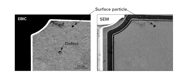
EBIC (Electron Beam Induced Current) imaging is an excellent complement to standard SEM imaging. EBIC can find defects that cannot be seen using standard SEM. Here EBIC reveals a ‘bright spot’ defect, not seen in the standard SEM image.
FURTHER DEFECT INVESTIGATION
EAG can find and characterize many types of defects. These include:
- Discoloration – XPS investigation of surfaces, GC/MS study of trapped gases
- Metal migration – FIB cross-section and investigation by Auger or STEM/EDS
- Voids – FIB cross-section and investigation by SEM
- Particles – surface imaging or FIB cross-section and investigation depending on size and possible organic content
- Cracks – FIB cross-section and investigation by SEM
- Delaminations – FIB cross-section and investigation by SEM
DEFECT ANALYSIS
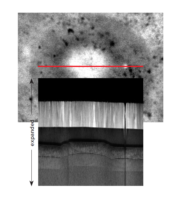
A closer view of the defect shows large and small bright spots in the EBIC image. A cross section of the defect was prepared using FIB. A TEM image of the defect cross-section is shown aligned on the same scale as the EBIC image. A pit defect is present under the small bright spot.
PIT DEFECT
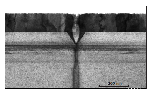
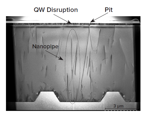
A TEM view of the pit defect shown above reveals v-shaped defects in the quantum well leading to pit formation in p-GaN that extended through the ITO to the surface.
Magnifying the TEM cross-section image vertically reveals a disruption in the quantum well epi-layer growth. The EBIC signal is stronger where the quantum well is in closer proximity to the ITO layer.
NANOPIPE DEFECT
Examination of the full TEM cross-section also reveals a nanopipe defect underneath the quantum well disruption shown above by EBIC and TEM.
GaN EPI-LAYER STRUCTURE
DISLOCATION DENSITY
Dislocation density at various stages of growth can be characterized by TEM. Plan view samples were prepared from this cross-section sample at locations 1, 2 and 3 as indicated.
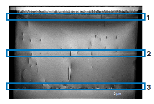

Plan view samples show dislocations (1) close to the QW layers, (2) in the middle of the GaN growth and (3) next to the sapphire substrate.
RAPID DEFECT TYPING
The character of dislocations can be determined using STEM imaging. By utilizing specific sample tilts, threading dislocations can be identified as having screw, edge, or mixed character.

SUPERLATTICE AND QUANTUM WELL
Aberration Corrected STEM can provide high resolution images and composition measurements.
EDS linescans from highlighted areas.
EPI-LAYER ANALYSIS
DOPING PROFILES
P type and n type dopants can be profiled by SIMS to measure concentration and distribution relative to the epi-layer structure.
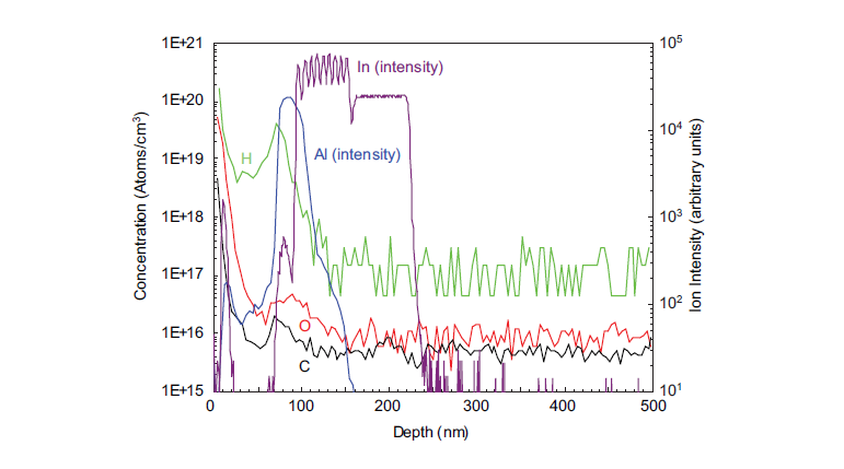
CONTAMINANT PROFILES
Contaminants can also be profiled by SIMS. These profiles can reveal growth issues layer by layer. Good detection limits for the ‘atmospheric elements’ (H, C, O) can be achieved with dedicated instrumentation.
Accurate quantification can be achieved using standards and controlled analytical procedures.
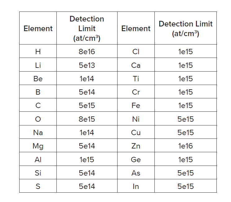
DETECTION LIMITS IN GaN
Very low detection limits for SIMS can be achieved using optimized analytical conditions and by using dedicated instrumentation.
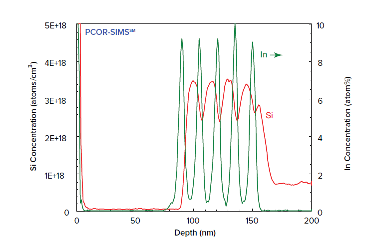
DOPANT PROFILE IN QW
High depth resolution SIMS can reveal the doping profile within the quantum well structure. The best quantification is achieved using ‘PCOR-SIMSSM’, a protocol that provides accurate quantification in all matrix layers.
EPITAXY PROCESS MONITORING — QUALITY CONTROL
DOPING PROFILES
SIMS depth profiles can be used to monitor reactor performance over time. Monitoring profile features such as concentrations and thicknesses can be a powerful method for process control.
SOFTWARE
EAG SIMSviewTM software for SIMS is routinely used to calculate dopant levels and layer thickness. We can customize and automate calculations to your specifications. Data is rapidly evaluated and can be compared to previously established benchmarks.
EAG EMviewTM software allows you to make measurements on SEM and TEM images. Brightness, contrast and gamma can be adjusted. Images can be rotated and annotated.
ADDITIONAL SERVICES
AlGaN – InGaN Composition: Improved accuracy by RBS. LM-80: Many environments for accelerated aging tests. Sapphire, SiC and other substrates: Surface contamination. Bulk contamination
STRESS BASED TESTING
Stress based qualification methodology provides a broad approach to identifying LED failure mechanisms and is a powerful tool to help engineers identify devices that may fail under a range of use conditions that LEDs. Thermal cycling, bias/humidity stress testing are conditions which many products experience and test conditions are designed to accelerate failures compared to field conditions to uncover potential issues at the device or packaged component and/or determine if the LEDs conform to industry standards.
BURN-IN TESTING
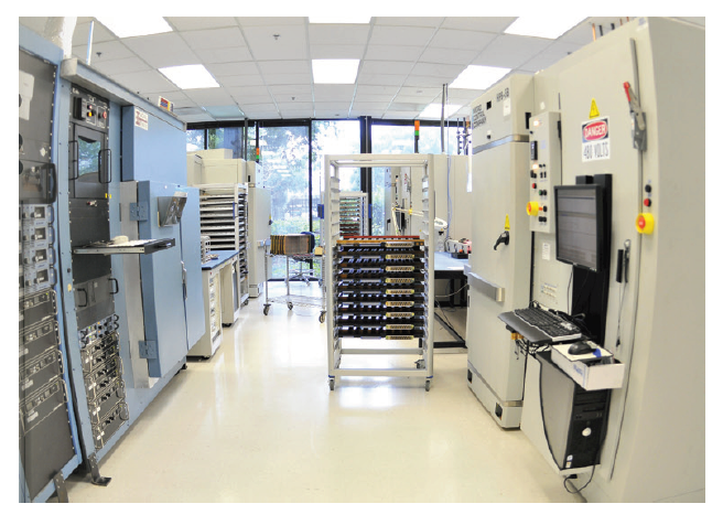
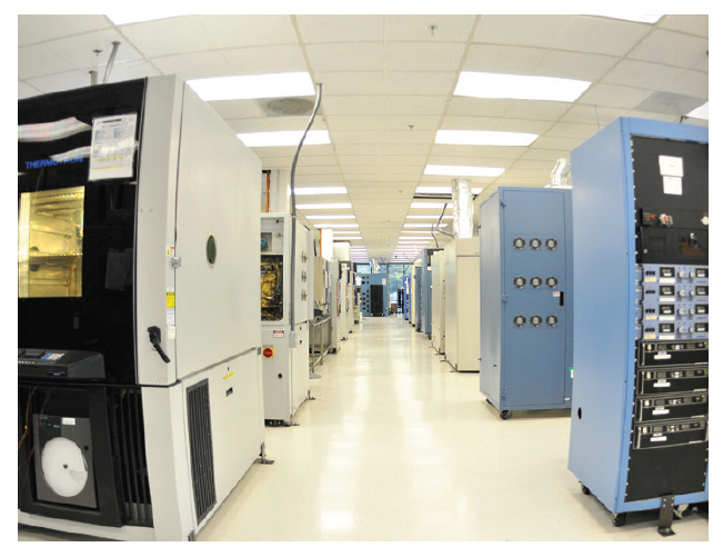
Burn-in testing is an important technique used to accelerate the conditions that stress LED devices to help you screen infant mortality and reduce your failure rate in the field. Our range burn-in equipment and team of experts can support a range of applications with excellent test control and monitoring. Our inhouse engineering team can design custom solutions to meet your specific needs and create solutions for the most challenging projects. We also have in-house PCB design to develop your burnin boards and fixtures, allowing us to support turnkey projects and deliver all the associated hardware required.
Would you like to learn more about LED Analysis?
Contact us today for your LED Analysis needs. Please complete the form below to have an EAG expert contact you.
