
Advances with Gallium Oxide
Gallium oxide has the potential to replace or substitute gallium nitride for power conversion in electric trains and vehicles.
Eurofins EAG Laboratories is the world-leading materials characterization and engineering resource for semiconductor testing. Our analytical and engineering services provide valuable answers for semiconductor clients as they develop new processes and materials, characterize ongoing processes and transfer processes to production.
EAG was initially founded to provide analytical services to semiconductor companies and continues to be a major industry sector. Our materials and microelectronic testing services are dedicated to providing the best information to add value for our customers in this sector. From prototype testing of devices in the ramp towards full scale production, to ensuring the purity of starting materials, we can help reduce development time and solve yield problems in the semiconductor manufacturing environment. How do I ensure the integrity of my critical materials supply chain?
Turn to EAG. WE KNOW HOW.
EAG offers a comprehensive suite of services for the semiconductor industry that can be used to investigate anything from devices to major components in semiconductor processing equipment. EAG applies a huge range of advanced surface and bulk materials analysis approaches that draw on our industry-leading array of microelectronics engineering services. We help our clients in semiconductor development and problem-solving. Here are just a few ways we can help
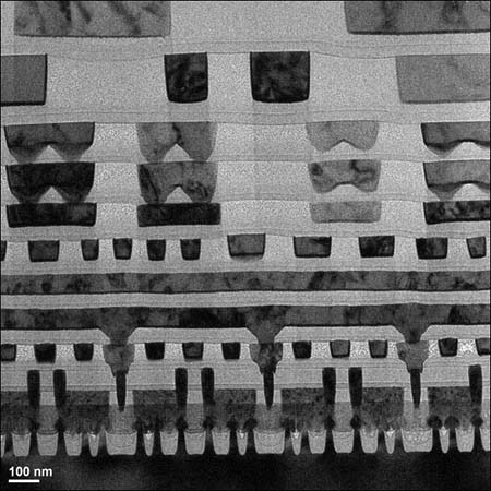
Microscopy techniques are essential to investigate sample micro-structure, morphology, particle size, particle coatings and defects in thin/thick films, bulk substrate materials, or to examine the cross-sectional structure of ICs.
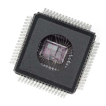
Our labs perform failure analysis on both integrated circuits, devices and final products. Failure analysis services range from Level 1 non-destructive examination to Level 3 fault isolation and root cause identification/analysis and characterization.
Investigation of materials-related issues includes the organic analysis of plastics/polymers, flux, lubricants and solder masks for identity, composition and purity, as well as elemental analysis of wire bonds, bond pads, leads and lead frames.
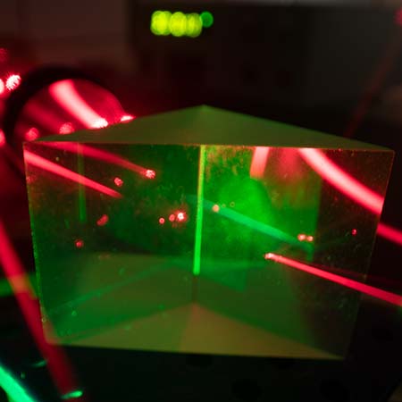
We can solve surface chemistry issues with adhesion and bonding, answer questions regarding surface cleanliness and perform investigations regarding morphology and topography of materials’ surfaces.
Identifying and locating trace level impurities in semiconductor devices through inspection of raw materials during key phases of manufacturing can aid in the identification and elimination of unwanted impurities in final products by careful characterization of supply chain components.
Secondary Ion Mass Spectrometry (SIMS) can measure dopant levels, detect very low concentrations of dopants and impurities, and can provide elemental depth profiles over a wide depth range from the extreme surface to the semiconductor substrate.
ESD testing services consist of HBM, MM and CDM. Both HBM and MM range from basic Level 1 testing to Level 4 comprehensive testing with detailed engineering diagnostics.
Reliability qualification helps our clients better understand wear-out mechanisms, detect design marginality combined with parameter drift and determine failure rates due to latent manufacturing defects.
Focused Ion Beam, or FIB circuit edit, services allow the customer to quickly cut traces or add metal connections within a chip at a small fraction of the cost of an entirely new lot of wafers in a fab.
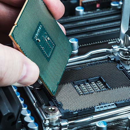
Small and large areas can be analyzed by multiple methods including AFM, XRR, profilometry and microscopy.
Thin films play an important role in the manufacture of all integrated circuits. EAG has a full suite of services available to characterize all critical aspect of novel thin films including their functionality and reliability that can be affected by the film’s composition, stress, uniformity, thickness, density, and grain structure.
Identifying particle contamination on all surfaces. All types of particles can be identified and measured: metallic, inorganic, organic, crystalline, amorphous, etc.
Our ATE test equipment and experienced team can support first silicon debug thru release to high volume production for a wide range of products, ranging from Digital to RF, including wafer sort and packaged part testing.
Access specialized methods to determine crystallinity, phase, texture and the effects of these on advanced semiconductor material performance.
Assessing cleaning efficacy by quantifying surface metals on wafer surfaces, identifying contamination such as particles, hazes, organic contamination or surface discoloration on wafers, optics and other critical surfaces.
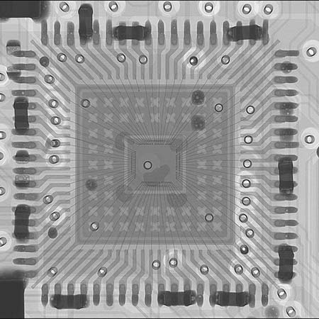
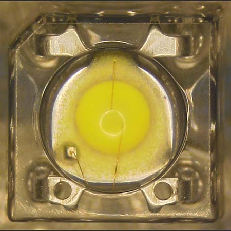
The most comprehensive and extensive range of state of the art advanced microscopy tools are available to analyze all current and future generation IC nodes.
Our team offers the engineering expertise to design, develop, test, analyze, and debug the most innovative products using ATE, system-level testing, reliability and IC-level failure analysis.
EAG’s experts offer litigation support for companies to confront potential threats to their valuable intellectual property, or patent infringement challenges related to semiconductor products claims.
For well over 40 years of Silicon Valley history, EAG has supported semiconductor equipment manufacturers in the design and test of showerheads, e-chucks, ceramics, plasma resistant coatings, and in assessng the purity of sputter targets.
We measure particles and TOC (Total Organic Contamination) on all parts that are used in the manufacture of Semiconductor processing equipment.
Using various techniques such as Trace Elemental Analysis sputter targets can be analyzed to determine the quality of the material that will be deposited onto a substrate.
Plasma resistant ceramic coatings are typically multi-layered structures that provide plasma erosion resistance, rigidity, conformability to substrate and thermal shock resistance.
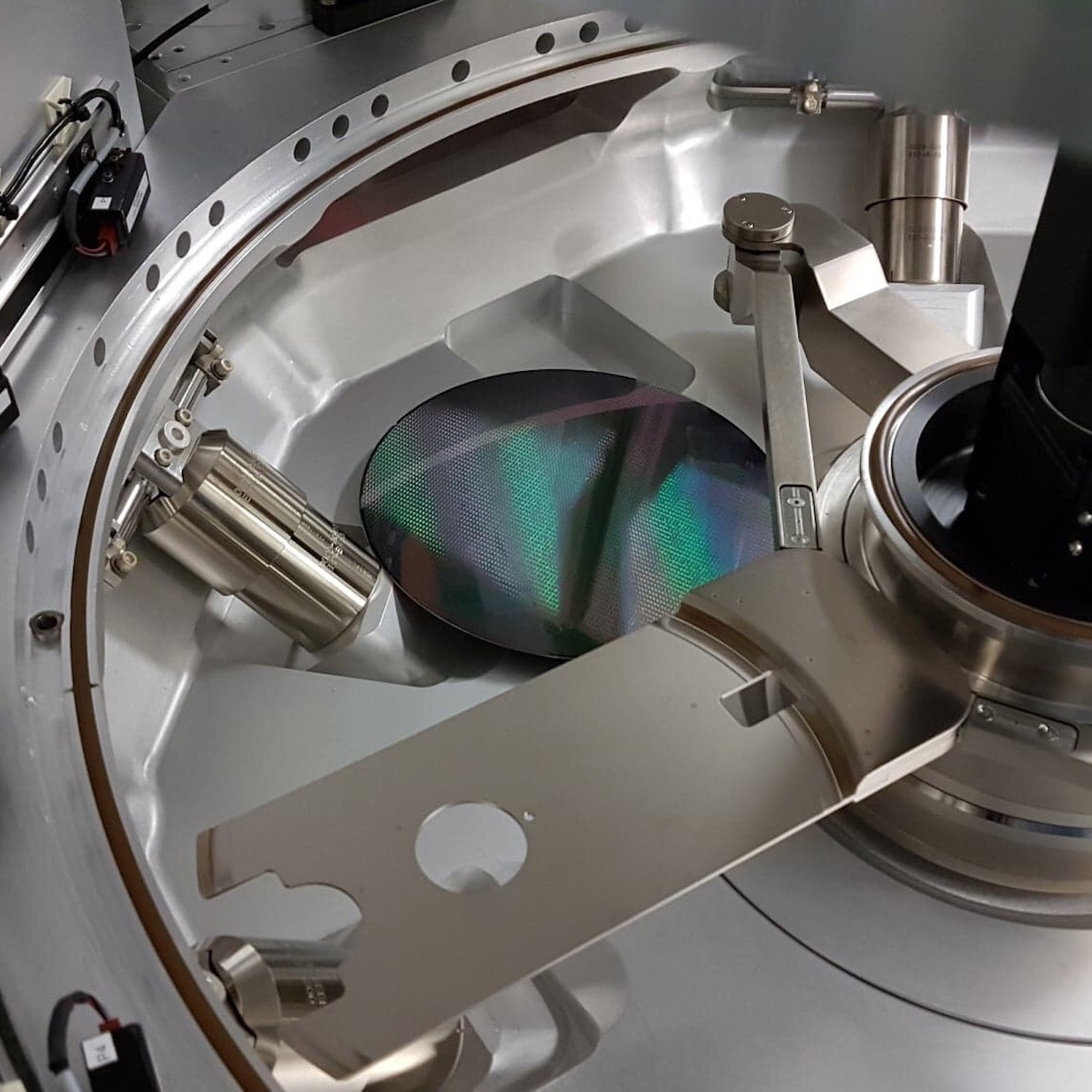
We can help you accelerate production release, as well as address capability and capital equipment gaps and manage the risk associated with semiconductor product development.
Contact us today for your semiconductor testing needs. Please complete the form below to have an EAG expert contact you.

Gallium oxide has the potential to replace or substitute gallium nitride for power conversion in electric trains and vehicles.

Cryo FIB uses a cold sample stage that can be controlled to -135°C making it it more suitable for temperature sensitive materials.
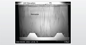
In the full webinar we introduce Characterization and Failure Analysis of Optoelectronic Materials and Devices
EAG has the timely accurate measurements and information you need to work with analysis of Atomic Layer Deposition thin films
To enable certain features and improve your experience with us, this site stores cookies on your computer. Please click Continue to provide your authorization and permanently remove this message.
To find out more, please see our privacy policy.