PCOR-SIMS Analysis of GaN HEMT Epitaxial Layers Grown on Silicon Substrates
Home » PCOR-SIMS Analysis of GaN HEMT Epitaxial Layers Grown on Silicon Substrates
AlGaN/GaN heterostructure field-effect transistors (HFETs) have been a subject of intense research and are now coming into production for use in high-voltage, high-power operation at microwave frequencies. Compared to similar devices made from GaAs-based materials, GaN has a larger peak electron velocity, higher thermal stability, and a larger band gap, all of which are very suitable as a channel material in microwave power devices. Further contributing to the performance of AlGaN/GaN-based HFETs is the ability to form two-dimensional electron gases (2DEG) with sheet carrier concentrations of 1013/cm2. These devices are more commonly referred to as High Electron Mobility Transistors (HEMTs).
An area of processing concern, however, is the substrate on which the 2DEG layers are grown. Growth on a GaN substrate would be ideal because of the exact lattice match between it and the layers being grown. This would mean that any GaN buffer layer grown to isolate the 2DEG from the substrate would not have to be very thick to avoid defects in the active region of the device. Unfortunately, GaN substrates cannot, at present, be grown in sufficiently large sizes to make them commercially viable from a cost standpoint.
Therefore, alternative substrates must be used. Single-crystal SiC is being used because of its electrical and thermal-conductivity properties, but mainly because it is very closely lattice-matched to GaN (3%). However, it, too, is quite costly. Sapphire substrates are less expensive but have poorer thermal conductivity (a disadvantage for high-power devices) and have an even higher lattice mismatch with GaN (13%). Therefore, silicon is now drawing much attention as a potential substrate because of its large base of established manufacturing tools and processes. However, Si is very highly mismatched to GaN which promotes the growth of many defects in the GaN grown thereon. This requires thick buffer layers of AlGaN to be grown between the Si substrate and the 2DEG-forming layers to reduce the defect density in this region of the device. An example of this is shown in Figures 1 and 2.
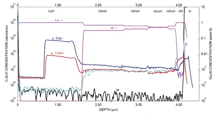
Figure 1 shows a Point-by-Point Corrected SIMS (PCOR-SIMSSM) depth profile of a complete GaN HEMT structure grown on a 150mm-diameter Si wafer. (The 2DEG region of the structure is almost imperceptible at the surface but we will address that later.) In this example, the buffer layer begins with an AlN layer. This material is not well lattice-matched to the Si underneath but it provides an insulating layer to isolate the layers above from the substrate.
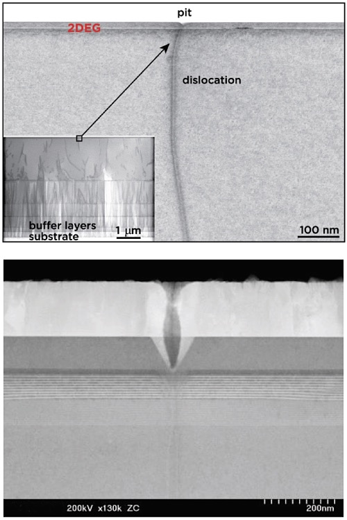
The AlN also acts as a seed layer upon which to grow successive layers of AlGaN with successively lower Al levels. The decreasing Al content lowers the defect density to acceptable levels by the time the GaN barrier layer is grown, as shown in the bottom left TEM micrograph of the sample in Figure 2. Note that the PCOR-SIMSSM analysis measures the various Al and Ga atomic fractions and layer thicknesses accurately.
Figure 1 also shows that the bottom half of the GaN barrier layer is doped with carbon. This carbon doping compensates the unintentional n-type doping by impurities (mainly Si and O as shown in the figure) in the AlGaN buffer and increases the breakdown field strength. However, the figure shows that the carbon doping in the GaN portion of the buffer at the edge of the wafer is a factor of ten higher than in the center. This will have considerable implications on the electric field reduction properties of the barrier layer at different locations across the 150mm wafer. However, one can see that the carbon content, as well as layer thicknesses, of the buffer layers are more similar between the center and edge of the wafer. The carbon level (as well as the Si and O levels) in the barrier layer is important because excessively high levels will lead to leakage in the devices.
In the vicinity of the 2DEG, carbon doping was reported to promote vertical leakage current, to cause degradation of both carrier density and carrier mobility of the 2DEG channel electrons, and to increase the dynamic on-resistance and current collapse, all of which are detrimental for device performance and reliability. In spite of the detrimental character of carbon doping on 2DEG and device properties, few reports have dealt with the residual carbon level in the active layers (AlN spike and AlGaN barrier layer). This is perhaps because measuring carbon in this near-surface region is severely hampered by surface pits that are always present due to threading dislocations originating deep in the buffer layer (reaching the surface) (see Figure 2).
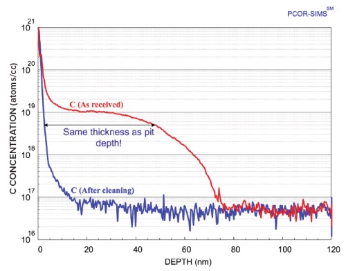
Carbon will become adsorbed on the air-exposed top surface and will not be entirely removed by the SIMS sputtering process until the entire pit is sputtered through. This artificially-deep carbon profile can totally obscure the real, important carbon distribution in the 2DEG region.
To circumvent this problem, we have developed a proprietary surface cleaning procedure that removes the vast majority of carbon from the surface thus eliminating the deep tail of the carbon profile (Figure 3). This allows us to measure the true carbon concentration in the AlGaN barrier layer just above the 2DEG as well as in the AlN spike just below the 2DEG.
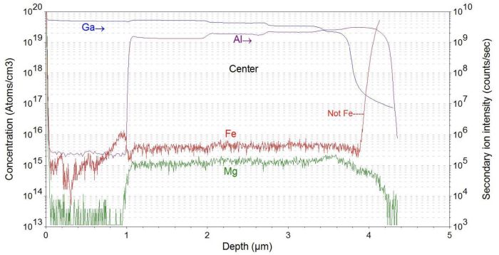
The buffer layer can also be doped with Fe and Mg. These can also be measured by SIMS with very low detection limits (Figure 4). Note the peak in the Fe profile just inside the GaN barrier layer. This peak is not present at the edge of the wafer, thus pointing out another difficultly in growing uniform layers across large substrates.
It is also important to control non-metallic impurity levels in the GaN barrier layer. For example, the Si level must be as low as possible in the GaN directly below the 2DEG because the device functions in the absence of dopants.
As shown in Figure 5, we can obtain Si detection limits in the mid 1014atom/cm3range; low enough to see the 2×10¹⁵atom/cm3 Si level just beneath the 2DEG.
Figure 5 also shows the levels of H impurities in the GaN barrier layer. Hydrogen can have deleterious effects on device reliability, so one tries to keep the H levels as low as possible. However, in this example, we see that the H level in the carbon-doped portion of the barrier layer is lightly elevated. This presumably arises from the source gas used for the carbon doping.
The region near the surface of the structure is where the 2DEG, which is responsible for the current flow in the device, is formed. The 2DEG forms here because of the conduction-band discontinuity between a thin, top-doped AlGaN layer and an undoped GaN layer. This creates a triangular quantum well in which electrons accumulate. This active region is exceedingly thin (20-30nm) and can be measured accurately by SIMS only with great care.
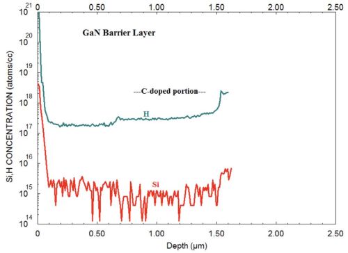
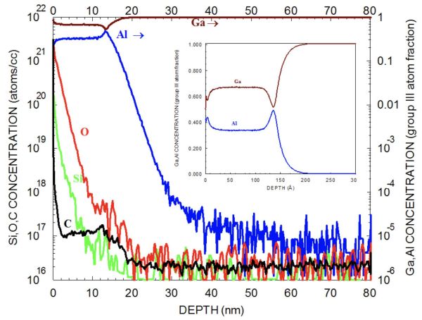
Figure 6 shows a PCOR-SIMS profile showing the Al which locates the AlGaN top layer along with the C, H, O and Si impurity of the 2DEG-forming region of a HEMT.
Since this layer is on the top of the structure, it is important to take measures to minimize the effects of the surface contamination that is always present on these air-exposed surfaces. In Figure 6, the carbon initially present on the sample surface was removed using our proprietary surface cleaning procedure which allowed the carbon-doping level to be measured in the AlGaN layer at a level of 1-2×10¹⁷atoms/cm3 within the top 15nm of the sample.
Figure 6 also gives the device engineer another important piece of information—the thickness of the AlGaN barrier layer. This is the layer through which the potential on the gate must act to control the density of electrons in the 2DEG and thus the conductance of the device. This can be seen in the linear-plot inset in Figure 6.
Figure 7 shows selected profiles of Figure 6 plotted on a linear scale instead of a logarithmic one, overlaid on a cross sectional TEM micrograph of the same region. The Al profile shows the location of the AlN delta layer which is included in the structure to improve the carrier mobility in the 2DEG by mitigating Coulomb scattering from the donors in the AlGaN.
We can see in the TEM micrograph that the actual width of the AlN delta layer is correctly measured by the full-width-half maximum (FWHM) of the Al profile above the constant level in the AlGaN layer, although the profile tails into the underlying GaN because of the surface pits shown in Figure 3.
The carbon profile is plotted to show the location of the doping with respect to the exact location of the interface (shown by the Al profile). TEM cannot be used to detect carbon, even with EDX (energy dispersive X-ray spectrometry) or EELS (electron energy loss spectroscopy).
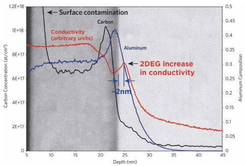
In addition, we show a profile (red) that is affected by the instantaneous surface potential from which the surface conductivity can be inferred. The 2DEG is formed just inside the GaN, and we can see from the plot that this is the exact depth at which the sample conductivity recovers after the profile passes through a zone of decreased conductivity just inside the barrier layer where the holes accumulate.
Conclusion
In conclusion, we have shown how Point-by-Point Corrected SIMS (PCOR-SIMS) can be used to determine accurate concentrations of matrix elements and dopants in GaN HEMTs and how these results can be of use in optimizing epitaxial layer growth and in failure analysis. If you have any questions, please feel free to contact EAG with your GaN HEMT analytical needs.
Would you like to learn more about Analysis of GaN HEMT Epitaxial Layers?
Contact us today for your SIMS analysis of GaN HEMT epitaxial needs. Please complete the form below to have an EAG expert contact you.