Reverse Engineering of Compound Semiconductors
Home » Reverse Engineering of Compound Semiconductor Optoelectronics
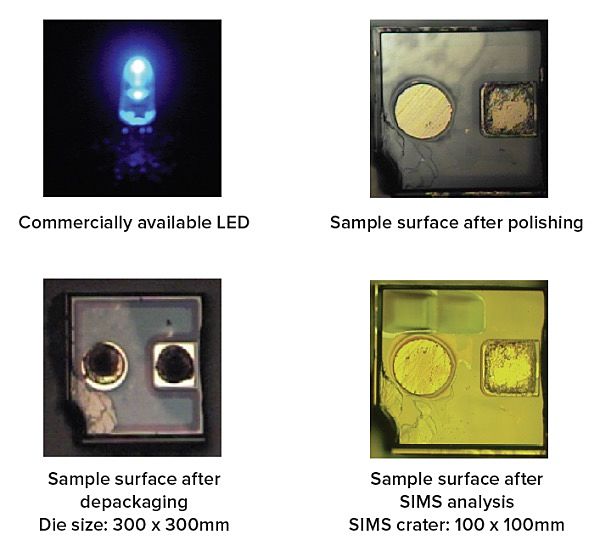
When information is required from a finished and packaged device, EAG Laboratories can depackage and deprocess the sample and then fully characterize it using various analytical techniques. Information that can be obtained includes:
- sample structure
- surface passivation layer presence (and thickness)
- active region thickness
- composition of the various layers
- dopant type (P or N), concentration and depth distribution
- composition (mole fraction) in ternary layers such as AlGaN or InGaN etc
- contaminant type, level and depth distribution
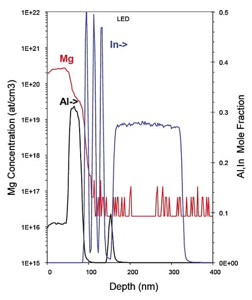
This example shows a SIMS depth profile of a blue LED device. SIMS showed the structure to be of the type: AlGaN/{InGaN/GaN}×3/AlGaN/InGaN/GaN, as seen from the Al and In profiles. The dopant (Mg and Si) distribution and concentration were also successfully measured.
Would you like to learn more about Reverse Engineering?
Contact us today for your reverse engineering of compound semiconductor needs. Please complete the form below to have an EAG expert contact you.