Atomic Elemental Mapping by Simultaneous Dual EELS and EDS
Home » Atomic Elemental Mapping by Simultaneous Dual EELS and EDS
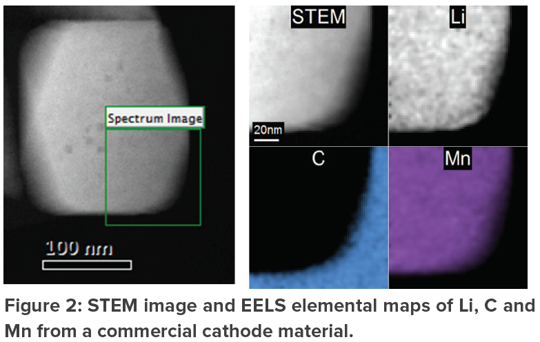
Electron energy-loss spectroscopy (EELS) and Energy dispersive spectroscopy (EDS), coupled with scanning transmission electron microscopy (STEM) provide local chemical composition along with structure information of materials. It was widely accepted that EDS is (only) good for heavy elements detection and EELS is (only) good for light elements. With the development of EELS spectrometers and EDS detectors, EELS and EDS are able to work on both light and heavy elements nowadays though each has its own strength and detection limits. EELS and EDS could work independently, but simultaneous EELS and EDS will provide a comprehensive chemical information.
With the advancements in aberration-corrected STEM, the electron probe size is now decreased to sub-angstrom level and at the same time, the current within the probe increases enormously. Such changes make it possible to collect enough signals for analytical analysis with a tiny probe, in other words to study not only the structure by also their chemistry atom-by-atom.
Would you like to learn more about Atomic Elemental Mapping?
Contact us today for your atomic elemental mapping needs. Please complete the form below to have an EAG expert contact you.