AFM Polymer Surface Modification
Home » AFM Polymer Surface Modification
Polymers are being used in an increasingly wider range of applications, particularly in the medical device industry. It is vital to understand polymer surface characteristics because many critical interactions between the polymer and its environment occur at the surface. For instance, the surface of a polymer used in a medical device is often the interface between the body and the device. By controlling the surface properties of the polymer, the medical device designer can enhance or inhibit various reactions of the body to the device. The interaction between the polymer and its environment depends in large part on surface composition and structure. Treatments such as spraying, vacuum deposition, and chemical or plasma etching have been developed to produce other desired surface characteristics and topographies.
Since surface composition and topography play such a large role in the performance of the polymer, precise surface characterization can be an important part in the rapid deployment of new materials or understanding of problems and behavior in existing materials. Atomic Force Microscopy (AFM), with its high-resolution surface mapping capabilities, can be a key component of that characterization.
SURFACE EFFECTS OF STRAIN AND PLASMA ETCHING
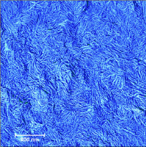
The images presented here demonstrate the effect of strain and oxygen plasma etching on an ethylene vinyl acetate film used in medical device packaging. The first image, Figure 1, shows a 4μm phase image of the as-received surface. To create a phase image the cantilever is oscillated near its resonance frequency and the phase lag between the cantilever and its driving force is plotted as a function of lateral cantilever position over the sample. The phase lag can be sensitive to physical property differences in the sample surface, as well as topography. The AFM phase image provides a detailed view of the polymer surface. The well-defined features in the phase image are probably the result of polymer lamellae that appear at the surface in slightly different orientations.
The second image, Figure 2, is a 5μm phase image of a different area of the same sample after the sample had been strained to the breaking point and the stress then released.
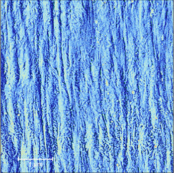
The strain direction runs from top to bottom in the image. Obviously, the surface has been modified by the applied stress. Combining this morphological information with detailed chemical analysis by techniques such as XPS or TOF-SIMS provides valuable information about the behavior of this sample. Since neither of these images required any type of sample preparation, the results are not affected by artifacts that may be created during a preparation process.
SAMPLE HISTORY
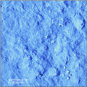
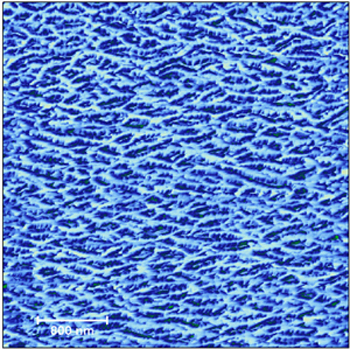
The history of a polymer surface sample can have an important effect on its behavior and performance. After the images shown in Figures 1 and 2 were acquired, the samples were etched in oxygen plasma for three different time intervals: 15 seconds, 1 minute and 3 minutes. Figures 3 and 4 show the effect of 3 minutes of plasma etching. It is obvious that the strained surface structure was affected to a much larger degree than the unstrained surface.
QUANTITATIVE ANALYSIS: SURFACE ROUGHNESS & PSD PLOTS
While being able to visualize the surface of a polymer is useful in itself, the ability to actually quantify physical characteristics can be important in some cases. Polymer surface roughness is an obvious parameter to measure from AFM data. However, while the roughness value of a sample surface can be useful, it can also be misleading. Two surfaces can have the same root mean square (RMS) roughness, but very different topographies. A power spectral density (PSD) plot of a surface can be a more effective tool in understanding and characterizing surface texture. The PSD is essentially the Fourier transform of a surface profile and shows the distribution of feature sizes on a surface. The power spectral density (PSD) plot of a surface can clearly reveal any periodic structures in that surface.
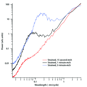
The RMS roughness value is calculated by taking the square root of the integral of the PSD over some frequency interval of interest. Figure 5 is a PSD plot that clearly shows how the strained-and-etched surface was affected by increasing the etch time. The PSD was calculated only in the y-direction to highlight the directionality of the surface structure. As expected from the images, the peak shifts to longer wavelengths with increasing etch time, indicating that the surface features are increasing in size. The increase in surface roughness with etch time is demonstrated by the increasing vertical position of the curves with etch time.
Would you like to learn more about AFM Polymer Surface Modification?
Contact us today for your AFM polymer surface modification needs. Please complete the form below to have an EAG expert contact you.