Auger Electron Spectroscopy (AES)
Home » Our Techniques » Spectroscopy » Auger
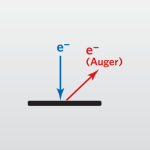
Auger Electron Spectroscopy (AES) is a surface-sensitive analytical technique that utilizes a high-energy electron beam as an excitation source. Atoms that are excited by the electron beam can subsequently relax, leading to the emission of “Auger” electrons. The kinetic energies of the emitted Auger electrons are characteristic of elements present within the top 3-10 nm of the sample.
This technique was named after French physicist Pierre Victor Auger in 1923. However, most people now recognize Austrian-Swedish physicist Lise Meitner as the person that first discovered that the emission of electrons from surfaces of atoms can create energy signatures.
The Auger Electron Spectroscopy technique uses a primary electron beam, typically in the 3 to 25 keV range. Atoms that are excited by the electron beam can relax through the emission of Auger electrons. The kinetic energies of the emitted Auger electrons are measured and are characteristic of elements present at the surface of a sample. The resulting spectrum is usually plotted as the derivative of the signal intensity vs. kinetic energy, with each element showing a unique “fingerprint” for elemental identification.
The electron beam can be rastered over a large or small surface area, or it can be directly focused on a small surface feature. This scanning electron beam also generates secondary electron (SEM) images that are used to locate the features of interest. Auger maps and linescans show the lateral distribution of elements on a surface, while depth profiles can reveal the composition as a function of depth.
AES Key Applications
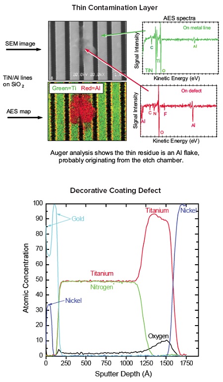
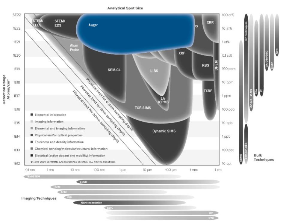
With a small electron beam diameter, AES is very useful when investing particles and small areas, as it has the ability to investigate sizes smaller than 25 nm. It also provides a good alternative when thin films are too thin for EDS analysis. AES can sample thin film stacks to a depth of a micron or more with sputtering.
Above all, AES is a semi-quantitative method, meaning that we typically provide results based on standard sensitivity factors provided by the equipment manufacturer. Where more accurate results are required, these can be obtained by looking at known compositions and comparing them to the unknown material.
The electron beam can be scanned over a variably sized area, or it can be directly focused on a specific surface feature of interest. This ability to focus the electron beam to diameters of 10-20 nm makes Auger Electron Spectroscopy an extremely useful tool for elemental analysis of small surface features. Other techniques that may also be considered are XPS and TXRF. When used in combination with a sputtering ion gun, Auger Electron Spectroscopy can also perform compositional depth profiling.
The electron beam can be scanned over a variably sized area, or it can be directly focused on a specific surface feature of interest. This ability to focus the electron beam to diameters of 10-20 nm makes Auger Electron Spectroscopy an extremely useful tool for elemental analysis of small surface features. Other techniques that may also be considered are XPS and TXRF. When used in combination with a sputtering ion gun, Auger Electron Spectroscopy can also perform compositional depth profiling.
Auger’s high spatial resolution capabilities and surface sensitivity make it the technique of choice for the following types of applications:
- Analyzing sub-µm particles to determine contamination sources
- Identifying defects in electronic devices to investigate failure causes
- Determining the oxide layer thickness of electro-polished devices
- Small-area depth profiling of bond pads on die
- Mapping of elemental distribution on discolored or corroded regions
- Cross-sectional analysis of buried defects in film stacks
- Identifying grain boundary contamination in metal fractures, fatigues and failures
- Integrity and uniformity of thin film coatings such as diamond-like-carbon (DLC)
Ideal Uses of Auger Electron Spectroscopy
- Defect analysis
- Particle analysis
- Surface analysis
- Small-area depth profiling
- Thin film analysis composition
- Metallurgical analysis
Auger Strengths
- High Spatial Resolution: ≥10nm minimum spot size
- Surface Sensitive; top 3-10nm
- Identification of all elements except H and He
- 2D and 3D elemental distribution of small areas
- Rapid analysis for elemental composition
- Can analyze up to 300mm wafers
Limitations
- Minimal chemical state information
- Insulators are difficult
- Samples must be vacuum compatible
- Detection limits of ~0.1% to 1% atomic
Auger Electron Spectroscopy Technical Specifications
- Signal Detected: Auger electrons from near surface atoms
- Elements Detected: Li-U
- Detection Limits: 0.1-1 at%; sub-monolayer
- Depth Resolution: 2-20 nm (in depth profiling mode)
- Imaging/Mapping: Yes
- Lateral Resolution/Probe Size: ≥10 nm
EAG has unmatched experience handling both routine and non-routine Auger analysis requests and, for many years, has used Auger Electron Spectroscopy to address a wide variety of industrial analytical applications.
EAG’s extensive Auger Electron Spectroscopy expertise has direct analytical benefits, whether we analyze sub-μm particles to determine contamination sources in wafer processing equipment or analyze defects in electronic devices to investigate the root cause of failures.
Finally, Auger analysis has extensive applications in metallurgical studies, including in the determination of oxide layer thickness of electro-polished medical devices, and EAG continually draws on its experience to help solve demanding problems from customers in many industry sectors.
Would you like to learn more about using Auger Electron Spectroscopy ?
Contact us today for your Auger Electron Spectroscopy (AES) needs. Please complete the form below to have an EAG expert contact you.