Scanning Electron Microscopy Cathodoluminescence (SEM-CL)
Home » Our Techniques » Imaging » SEM-CL
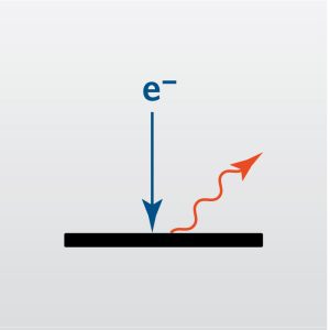
Cathodoluminescence (CL) is electromagnetic radiation, or light, ranging from visible (VIS) to near-infrared (NIR) created by the interaction of high-energy electrons (cathode rays) with a luminescent material. The light that is emitted carries very specific information about the optical and electronic properties of the sample.
Using a specialized Scanning Electron Microscope (SEM) that has visible light collection, corresponding sample structure (SE) and CL emission maps can be acquired simultaneously with sub-micrometer resolution. In some cases, the CL spatial resolution can be as good as 30-50 nm. CL mapping can be performed on both cross-sections (XS) or in plan-view (PV) to characterize a sample’s localized composition, doping, structure and defects, all with very high spatial resolutions.
Ideal Uses of SEM-CL
- Materials characterization – crystalline defects, bandgap determination, intra-bandgap trap states, composition, dopants
- Semiconductor failure analysis – defect localization within devices for deeper failure analysis (FA)
Strengths of Cathodoluminescence
- Provides highly localized information about materials optical and electronic properties
- Does not require electrical connections
Limitations of Cathodoluminescence
- Requires a luminescent material – semiconductors, polymers, insulators, metal photonic structures
- Smaller samples required, no full wafers larger than 1” dia – 3 mm height restriction
- Large amounts of topography, especially non-uniform surface roughness, can make CL collection and contrast interpretation more difficult. Smooth samples are preferred
- Thick (μms) metal contacts on the surface of a device must be removed before analysis. This can be often done by careful chemical etching or in specific regions by Focused Ion Beam (FIB)
- Localized dopant characterization is possible but requires careful choice of standards
SEM-CL Technical Specifications
- Signals Detected: Simultaneous Secondary Electrons (SE) and Cathodoluminescence (CL)
- Wavelengths Detected: 250-1500 nm
- Imaging/Mapping: Yes
- Lateral Resolution: Typically varies from 20-500 nm depending on SEM conditions and sample composition/topology
Related Resources
Would you like to learn more about using SEM-CL?
Contact us today for your Scanning Electron Microscopy Cathodoluminescence needs. Please complete the form below to have an EAG expert contact you.