Electron Backscatter Diffraction (EBSD) is a technique that is uniquely suited to characterize crystallographic properties of your samples. Proprieties such as: grain size, grain shape, grain orientation, grain boundary misorientation, spatial distribution of phases, local deformation and texture can all be characterized by this technique.
EBSD Analysis is a great complement to the excellent capabilities of our X-ray diffraction (XRD) services. While our XRD tools and staff can provide unparalleled information on phase ID, nanocrystalline grain size, thin film thickness and textures; the new capabilities available by EBSD will provide spatial information, help to visualize the microstructure and add to a complete description of your crystalline samples.
Ideal Uses of EBSD
Visualization of microstructure with spatial coordinates
Characterization of texture in exact locations such as near welds or on semiconductor bond pads
Characterization of grain size & texture as it related to finish quality in sheet steel and Al
Measurement of large grains, without the error associated with LM
Characterization of special grain boundaries, such as CSL’s and twins
Measurement of grain misorientation
Characterization of deformation by examination of intragrain misorientation and grain aspect ratio
Characterization of epitaxially grown thin films
Characterization of in-depth texture, by examining cross sections
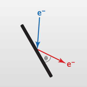
EBSD – Electron Back Scatter Diffraction is a technique using the electron beam of a SEM to differentiate the crystallographic orientations of grains on a sample surface. From EBSD we obtain:
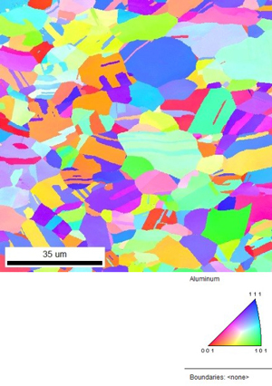
Grain orientation
Grain size
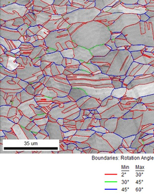
Misorientation between grains
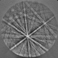
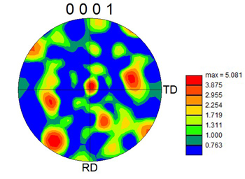
Pole figures and maps
Electron Channeling Pattern Kikuchi Map
Inverse pole figure map
Grain boundary map
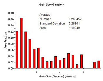
Grain size distribution
Pole map
Strengths
Accurately provides spatially resolved grain size and phase information from several 10s of nm to several 10s of mm.
Provides texture information from localized area.
Provides grain boundary angle information.
Can be used for failure analysis.
Limitations
The phase information needs to be known a-priori.
Cannot analyze amorphous materials.
Cannot distinguish phases of similar crystal structures (need to use EDS-EBSD technique).
High-quality polished surface is required.
EBSD Technical Specifications
Signal Detected: Diffracted electrons
Elements Detected: All elements, assuming they are present in a crystalline matrix
Detection Limits: Grain size >80 nm
Quantitative analysis: Grain size and related measurements: ~10%
Would you like to learn more about using Electron Backscatter Diffraction (EBSD)?
Contact us today for your Electron Backscatter Diffraction (EBSD) needs. Please complete the form below to have an EAG expert contact you.
To enable certain features and improve your experience with us, this site stores cookies on your computer.
Please click Continue to provide your authorization and permanently remove this message.