Home » Quantification of Ultrathin Layers by AC-STEM-EDS
Recent advances in thin film technologies, and their materials properties, have led to significant characterization challenges. For instance, the characterization of quantum well structures on samples with anti-reflective textures, patterned substrates, or the presence of crystalline defects can be very complicated ultimately preventing the access to the basic information required. However, the accurate determination of ultrathin layer composition, thickness and morphology are critical for process development, evaluation of device quality or failure analysis. At EAG Laboratories we have developed a specific analytical protocol for such challenging characterization problems on these devices.
In this application note we show the effectiveness of thin layer quantification by Aberration Corrected Scanning Transmission Electron Microscopy (AC-STEM) coupled with an energy dispersive x-ray detector (STEM-EDS) for GaN-based samples.
RESULTS AND DISCUSSION
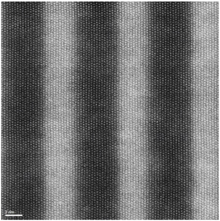
As can be seen in Figure 1, the AC-STEM provides highly detailed images of the sample. This image clarity is not possible with traditional STEM or TEM images. With image resolution better than 1.4Å, AC-STEM can provide unparalleled layer thickness accuracy and detail.
In addition to excellent image quality, the AC-STEM coupled to an advanced x-ray detector allows for reliable quantification of GaN-based materials.
Figure 1 AC-STEM Z-contrast image of GaN:InGaN multilayer stack. The AC-STEM shows clear atom stacks (round spheres) that indicate superb image resolution.
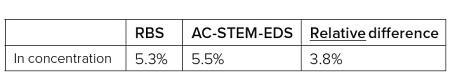
As an example of the accuracy that can be obtained by AC-STEM-EDS, Table 1 shows the results comparing the measured values by AC-STEM-EDS and by Rutherford Backscattering Spectrometry (RBS). RBS is used to create reference standards and is considered to be one of the most accurate analytical techniques for thick films. The agreement between RBS and AC-STEM-EDS is within the expected RBS measurement uncertainty of 5% (relative).
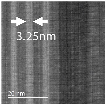
Figure 2 AC-STEM image from an ultrathin layer in an LED device.
Table 1 In concentration on a InGaN thick film standard sample.
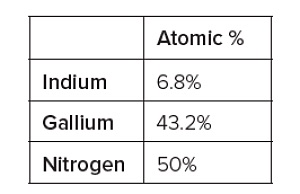
Table 2 Elemental concentration from layer in Figure 2.
Table 2 shows the quantitative composition measured from a 3.25nm layer in an InGaN structure using AC-STEM-EDS under the same analytical conditions used for the RBS standard. For many important material systems (including III-V, III-Nitride, and II-VI devices) quantified composition cannot be realized by any other method, such as SIMS. It is important to note that because the analytical conditions on the calibration standard and the thin film are the same, the accuracy of the data in Table 2 is identical to that obtained from the bulk film shown in Table 1.
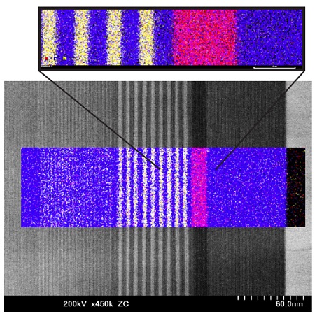
In addition to excellent quantitative results on these challenging samples, AC-STEM-EDS can provide vivid images of elemental distributions as shown in Figure 3. These maps can provide unique information regarding sample composition and defect analysis, all with nm scale resolution.
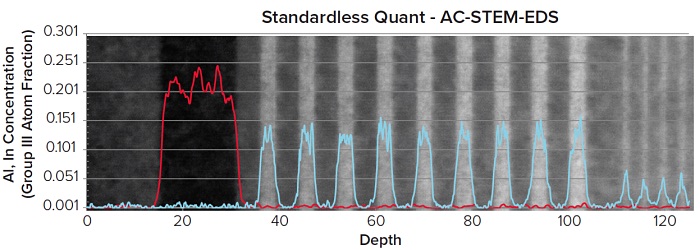
Linescans are another method of measuring elemental distributions that can provide an additional level of information. Figure 4 shows a line scan of the same sample, showing the atomic fractions of Aluminum and Indium in the GaN sample. Note that the thinnest Indium layers on the right side of the scan are on the order of 1.5nm thick. The quantification accuracy of these layers has not yet been determined. However, in the thicker layers (3.25nm) the concentration values are valid due to the previously mentioned analytical conditions and the probe size being significantly smaller than the film thickness.
Figure 3 Al (red), Ga (blue) and In (yellow) distributions in a InGaN quantum well structure.
Figure 4 Standardless quantitative line scan of Al (red) and In (blue) atom fractions. The wide variations in atomic fraction are due to the high pixel resolution required for this data type. For quantitative analysis, as shown in Tables 1 and 2, the data are collected in a way to significantly improve these statistics.
SUMMARY
We have shown in this application note that it is possible to accurately quantify ultrathin layers of a GaN-based device. This method may be extended to investigations on other III-V, III-Nitride, and II-V materials. This AC-STEM-EDS data, coupled to SIMS profiles are essential to understand the complex material systems that are now commonplace in todays advanced electronic devices.
Would you like to learn more about Quantification of Ultrathin Layers?
Contact us today for your quantification of ultrathin layers by AC-STEM-EDS. Please complete the form below to have an EAG expert contact you.
To enable certain features and improve your experience with us, this site stores cookies on your computer.
Please click Continue to provide your authorization and permanently remove this message.