EDFAS Silicon Valley EFA Workshop: An in-depth look
December 3, 2025
Discover the latest in semiconductor failure analysis through expert presentations and guided lab tours.
December 3, 2025
Discover the latest in semiconductor failure analysis through expert presentations and guided lab tours.
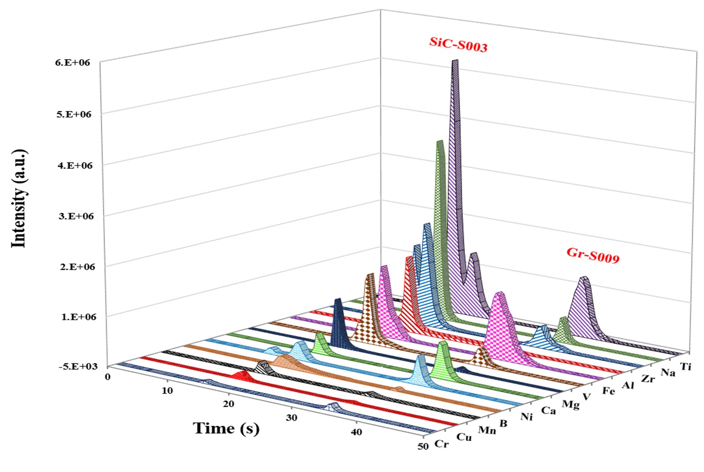
Electrothermal vaporization (ETV) coupled with ICP-OES is an exceptionally sensitive solid sampling technique for purity verifications.
Demand for compound semiconductors has rapidly grown recently. During this live event we answered questions surrounding the Materials Characterization of GaN HEMT power transistors.

XRD analysis can be used on many scientific and technology-based applications where you may want to identify the crystalline material in a very small area or volume, such as glass defects or inclusions, integrated circuits, LEDs and more.

VCSELs have several advantages, such as a higher modulation speed, which make them great for technological innovations.

May 15, 2024
Check out our online symposium presented by EAG Laboratories and Exponent!
To enable certain features and improve your experience with us, this site stores cookies on your computer. Please click Continue to provide your authorization and permanently remove this message.
To find out more, please see our privacy policy.