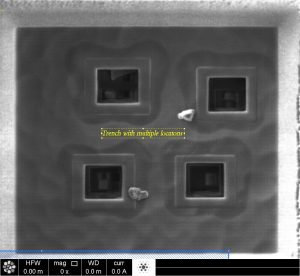
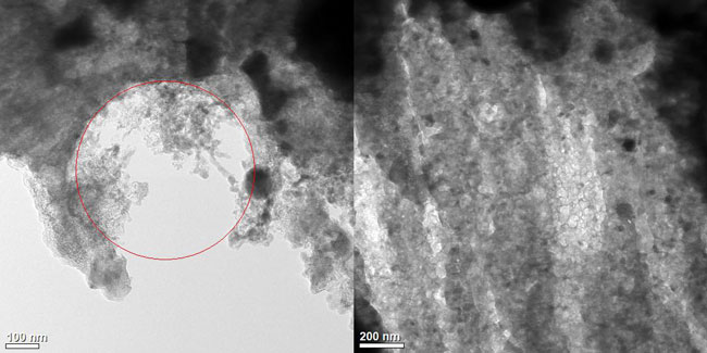
SIMS Characterization of Atomic Layer Deposition in Electronic Applications
Atomic Layer Deposition technology aids in the demand for computational advancement in the microelectronics industry.
Home » When Temperature Matters – Cryo TEM
As innovation in technology propels us into the future, the importance of new materials continues to increase. These materials are used to develop and enhance new products. Analytical testing can help to better understand the composition of a new material or to help solve a failure during product development or after product release.
In our blog, ‘A Solution for Sensitive Materials – Cryo FIB’, we discussed how materials are not equal in how they react to certain techniques or environments. Some materials are more sensitive to air and temperature, making them more prone to damage during analysis. In addition to Cryo FIB, Eurofins EAG also offers Cryogenic Transmission Electron Microscopy (Cryo TEM) which provides another solution for sensitive materials. Cryo FIB is used to prepare samples for TEM and can provide imaging using SEM. Cryo TEM can provide even better resolution and additional information such as chemical state and elemental mapping using Electron Energy Loss Spectroscopy (EELS) and Energy Dispersive X-ray Spectroscopy (EDS).
Cryo TEM involves performing Transmission Electron Microscopy (TEM) analysis while keeping the sample at cryogenic temperatures, around -170°C. For years, Cryo TEM was primarily used within the biological community to study biomolecule structures. The lower temperature helped to prevent damage to the samples from the electron beam. With the development of new batteries, similar beam damage problems can occur which has piqued new interest in Cryo TEM.
A hole (circled in red, left image) can be drilled in the sample (lithium containing materials) right after the electron beam shines on the sample inside TEM at room temperature, which makes it impossible to study the materials.
On the other hand, once the sample is cooled down to cryogenic temperature, the sample is very stable, and no obvious change is observed after 30 mins (right image).
With our many years of materials expertise and extensive research, Eurofins EAG can identify material problems to help you launch your product faster and more efficiently. Contact us today to learn how we can help.
Atomic Layer Deposition technology aids in the demand for computational advancement in the microelectronics industry.
All materials have trapped gasses inside. Learn how EAG utilizes Evolved Gas Analysis to analyze what gasses are being released.
Essentials of Particulate Testing: USP <788> and AAMI TIR42 While there are many standards available for particulate testing, USP <788> and AAMI TIR42 are the most important. This is especially
May 15, 2024
Check out our online symposium presented by EAG Laboratories and Exponent!
To enable certain features and improve your experience with us, this site stores cookies on your computer. Please click Continue to provide your authorization and permanently remove this message.
To find out more, please see our privacy policy.