Extractable & Leachable Studies for Consumer Products Webinar
In this webinar we introduce Extractable and Leachable tests which identify chemical components that can migrate out of a product.
Home » VCSELs as a Critical Component for the Consumer Electronics 3D Sensing Market
Three-dimensional (3D) technology is a considerable scientific breakthrough. It is a depth-sensing technology that augments camera capabilities for facial and object recognition. The process of capturing a real-world object’s length, width, and height with more clarity and in-depth detail that can be achieved using several different technologies.1 The adoption of this technology has been slow over the past 10 years but is now witnessing a robust expansion driven by factors such as technological advancements and a growing demand for smart devices. The 3D sensor market size is estimated to reach $9.4 billion by 2026 and is expected to grow at a CAGR of 28.1% from 2021 to 2026.2 Additionally, the US consumer electronics market is projected to reach $401 billion by 2027, with a compound annual growth rate (CAGR) of 7.5% during the forecast period.3
3D sensing technology is incorporated into our everyday lives from iris scanning, video conferencing, gaming, facial recognition, secure

banking, collision detection/warning, and 3D picture/video on mobile phones. It has expanded in the robotics industry and is increasingly used in consumer, automotive, drones, and industrial applications.
Vertical-cavity surface-emitting lasers, or VCSELs, play a major role in the consumer electronics 3D sensing industry. Companies utilizing a short-wave infrared (SWIR) VCSEL, a technology that reduces interference from sunlight and ambient light while mitigating white-spot phenomena, will help drive VCSEL prices up to see a market rebound. As a result of consumer electronics, the 3D sensing VCSEL market is forecasted to rise at a CAGR of 11% from 2023 to US $1.4 billion in 2028.4
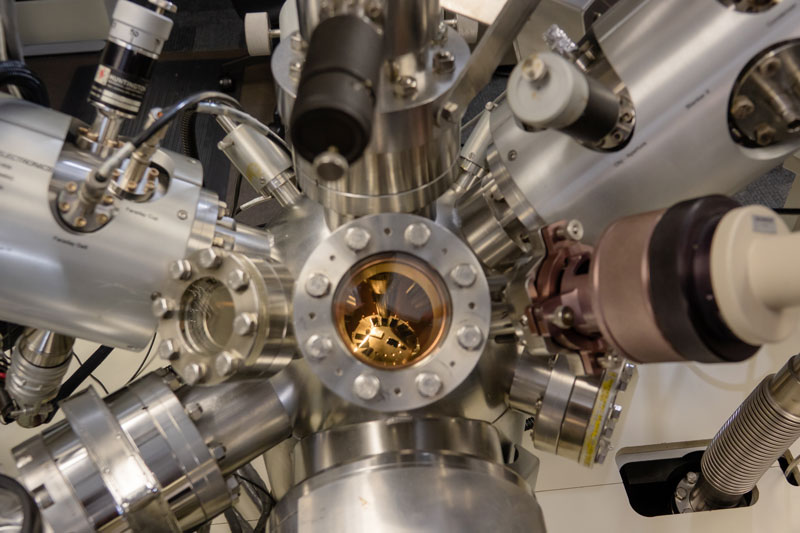
The PCOR-SIMSSM technique pioneered by EAG is an EAG proprietary technique that can measure layer thickness, composition, and doping profiles more accurately than a regular SIMS analysis, where calibration with respect to alloy composition is not made at every data point. PCOR-SIMSSM can provide:
PCOR-SIMSSM continues to be a valuable resource for EAG customers to achieve a more accurate analysis and to provide the data they need to create sophisticated products efficiently.
EAG is the industry standard for SIMS analysis, offering the best detection sensitivity along with accurate concentration and layer structure identification. No other analytical laboratory can match EAG’s depth of experience, as well as dedication to research and development in the SIMS field. We have the highest number of SIMS instruments worldwide (more than 50 SIMS instruments), highly qualified scientists, and the world’s largest reference material library of over 8,000 ion-implanted and bulk-doped standards for accurate SIMS quantification. EAG has been doing SIMS analyses for over 40 years; longer than any other commercial laboratory.

In this webinar we introduce Extractable and Leachable tests which identify chemical components that can migrate out of a product.

July 30, 2024
Please join us for coffee and conversations! Enjoy a cup of coffee and refreshments as you get to know our technical experts.
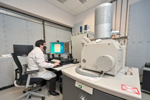
SEM equipped with EDS can capture detailed images and identify elements simultaneously on the surface of samples.

The term ‘rare earth elements’ (REEs) is a misnomer and better refers to the relatively rare ores REEs are extracted from; rare earth elements are all around us!
To enable certain features and improve your experience with us, this site stores cookies on your computer. Please click Continue to provide your authorization and permanently remove this message.
To find out more, please see our privacy policy.