Analysis of GaAs pHEMT & GaN HEMT Webinar
In the full webinar we will focus on the PCOR-SIMS Analysis of GaAs pHEMT and GaN HEMT using Secondary Ion Mass Spectrometry
Home » The Crucial Role of Warpage Analysis
In the world of engineering and manufacturing, precision isn’t just a goal; it’s a necessity. Among the challenges encountered by engineers, one significant hurdle is the warping of materials and components. The occurrence of warpage events can significantly impact the performance and reliability of products. In this complex field where accuracy is crucial, tackling material and component warping is vital to meet top standards in quality and functionality in our advancing technological age.
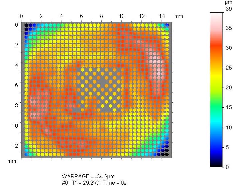
Warpage Analysis serves as a valuable tool for measuring the warpage and deformation experienced by products under thermal stresses. This analysis provides a detailed 3D topographical profile, particularly relevant in the realms of materials engineering, mechanical engineering, and manufacturing. Warpage commonly arises from factors like thermal stress, uneven cooling, or internal stresses during the manufacturing process.
A significant concern is the potential for deformation caused by a mismatch in the coefficient of thermal expansion (CTE) within a device or PCB. This misalignment can lead to warping during the reflow process or thermal expansion during regular operation, resulting in failures at the interconnects.
Warpage Analysis excels in offering In-Situ measurements of warpage and deformation, providing critical insights for optimizing heat dissipation strategies in various industries.
Warpage Analysis is a versatile tool used at different stages of product development. It’s valuable in research and development, process control, and designing manufacturing processes. Acting as a quality control measure, it ensures products meet standards and assists in failure analysis for issue identification and resolution. Its usefulness extends throughout the product lifecycle, contributing to the optimization and reliability of manufacturing and design processes.
The need for Warpage Measurement has risen in modern manufacturing due to new factors. Changes like using lead-free solder, smaller and denser balls, thinner components and printed circuit boards (PCBs), and larger ball grid array (BGA)-type devices make precise warpage measurement crucial. Moreover, the demand for increased heating dissipation in these advanced setups highlights the vital role of Warpage Measurement in securing the reliability and performance of contemporary electronic components and systems.
EAG Laboratories has partnered with Insidix to provide a Compact-3. This TDM tool uses the fringe projection technology for non-contact, full-field acquisition of 3D topographies with submicron resolution. TDM technology allows our clients to understand and predict the potential of warpage variation of electronic devices during process steps such as reflow or the complete life cycle of the product. After analyzing a sample, the TDM software provides intuitive results in the form of 3D plots, vector diagrams and 2D profiles.
Our capabilities include:
Contact us today to learn more.
In the full webinar we will focus on the PCOR-SIMS Analysis of GaAs pHEMT and GaN HEMT using Secondary Ion Mass Spectrometry
Nanoprobing is crucial for understanding advanced semiconductor devices, finding faults, and conducting thorough failure analysis.
EAG provides essential services for common devices and platforms that are instrumental to the electronics industry. These include artificial intelligence, ASICs, PCB Assembly, and Discretes.
EAG Laboratories provides clients with answers to these questions and more with testing support for every stage of the supply chain.
To enable certain features and improve your experience with us, this site stores cookies on your computer. Please click Continue to provide your authorization and permanently remove this message.
To find out more, please see our privacy policy.