Failure Analysis in a Complex World Webinar
In this webinar we show how EAG troubleshoots electronic system failures using a multidisciplinary approach
Home » Navigating Consumer Electronics Development: Early Stage Materials
In the fast-paced world of consumer electronics, every stage of development is critical to success. Eurofins EAG Laboratories stands as a reliable partner, offering extensive support tailored to the unique needs of each client. From the initial conceptualization to the delivery of the final product, our expertise plays a crucial role in shaping the future of consumer electronics.
Contamination or the presence of thick oxide layers on bond pad surfaces can lead to poor adhesion and electrical connectivity with the wire or ball. Auger analysis helps identify bonding issues by monitoring bond pad cleanliness and measuring oxide layer thickness. In a case study, Auger analysis found a higher concentration of fluorine contamination on the bond pad surface. This discovery prompted an investigation, revealing that a foam material used for sample separation at the wafer level was the source of fluorine contamination, reacting with the bond pad surface.

In the early stages of materials development for consumer electronics, a myriad of technologies comes into play, including semiconductors, MEMs & NAND structures, plastics, glass, and various raw materials. To facilitate this crucial phase, Eurofins EAG Laboratories provides a range of essential services:

Advanced Microscopy:
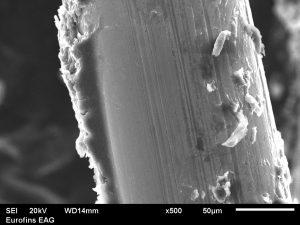
In the realm of early-stage materials development, advanced microscopy becomes the lens through which intricate structures come to light. Our experts meticulously examine sample micro-structure, morphology, particle size, and the presence of coatings and defects in thin/thick film or bulk substrate samples. This in-depth analysis lays the groundwork for understanding the fundamental characteristics that will define the material’s performance.
Coatings Analysis:
Coatings play a pivotal role in the functionality and durability of consumer electronics. Eurofins EAG Laboratories addresses challenges associated with coatings, including paints and adhesives. Our services encompass depth-specific distribution measurements and comprehensive chemical survey characterizations. This detailed analysis provides a roadmap for overcoming potential obstacles and optimizing coating performance.
Materials Characterization:
Our team investigates critical aspects such as organic analysis of plastics/polymers, flux, lubricants, and solder masks. Elemental analysis of wire bonds, bond pads, leads, and lead frames offers a holistic understanding of the material’s composition. This exploration is fundamental to shaping materials that meet the stringent requirements of the consumer electronics industry.
Purity Services:
Our purity services are designed to determine trace and ultra-trace level chemical impurities, ensuring that materials adhere to the highest standards of quality. Over the last thirty years, EAG has established an extensive range of trace analysis services. This suite incorporates advanced analytical techniques, a comprehensive database of reference materials, a highly educated staff applying scientific expertise for effective problem-solving, and a robust commitment to data security and intellectual property confidentiality.
At Eurofins EAG Laboratories, we understand that success in consumer electronics hinges on the precision and reliability of materials. Our early-stage support services are designed to empower developers, ensuring that every material meets the stringent requirements of the industry. Contact us to learn how we can assist in your consumer electronics needs.

In this webinar we show how EAG troubleshoots electronic system failures using a multidisciplinary approach

In this webinar we introduce latch-up testing which is relevant for CMOS devices with high static power dissipation.

TEM, STEM and AC-STEM techniques deliver high resolution images providing a detailed view of a material or product.

This webinar covers FDA regulation of medical devices, the most commonly used test standards, and custom testing at Eurofins EAG Laboratories.
To enable certain features and improve your experience with us, this site stores cookies on your computer. Please click Continue to provide your authorization and permanently remove this message.
To find out more, please see our privacy policy.