Analytical Approaches for Food & Beverage Webinar
In this webinar we introduce the analytical approaches for solving food and beverage challenges including contamination.
Home » Materials Characterization for a Semiconductor Testing Customer
Many consumers are not aware of the tiny chips powering their everyday electronics called semiconductors. These little devices have paved the way for unbelievable advancements in innovation, technology, and have dramatically influenced how we function daily. According to the 2022 State of the U.S. Semiconductor Industry report “over the past three decades, the semiconductor industry has experienced rapid growth and delivered enormous economic impact. Chip performance and cost improvements made possible the evolution from mainframes to PCs in the 1990s, the Web and online services in the 2000s, and the smartphone revolution in the 2010s. From 1995 to 2015, an estimated $3 trillion in global GDP has been directly attributed to semiconductor innovation, along with an additional $11 trillion in indirect impact. Semiconductors are essential to our modern world which is why the long-term market demand remains strong”1 (Association).
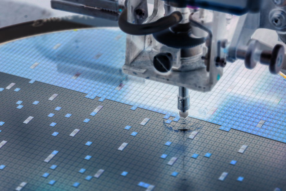
Eurofins EAG Laboratories (EAG) is the world-leading materials characterization and engineering resource for semiconductor testing. EAG’s material and microelectronic testing service is dedicated to providing the best information from ensuring the purity of starting materials, to prototype testing of devices in the ramp up towards full-scale production. With our analytical expertise EAG can help clients ensure the integrity of their critical materials supply chain while also helping to reduce development time and solve yield problems in the semiconductor manufacturing environment.
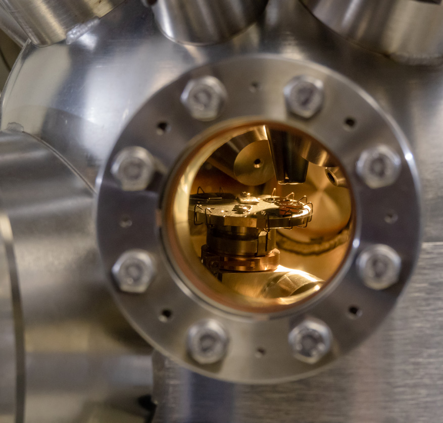
A large semiconductor equipment manufacturer was trying to bring a new and advanced technology to market, but the device wasn’t performing as expected – it kept failing before its expected lifetime. Their customer was interested in a demonstration as soon as possible so a prompt solution was imperative. To provide a higher level of confidence, the semiconductor company reached out to EAG, an independent and non-biased materials testing laboratory, to provide additional analysis. After performing Secondary Ion Mass Spectrometry (SIMS) analysis on the technology, EAG scientists were able to determine the root cause of the issue(s), provide a detailed report to the semiconductor company, and work with them on mitigating the problem.
Working with a company that has decades of experience, and technical experts who have unique knowledge, is a great benefit. Not only can EAG leverage their extensive reference materials database of over 8,000 unique calibration standards, but their experts also provide suggestions which utilize additional characterization
techniques to provide a comprehensive solution for a given problem. EAG can work with speed and efficiency to meet the tight deadlines of their clients.
EAG offers a comprehensive suite of services for the semiconductor industry that can be used to investigate anything from devices to major components in semiconductor processing equipment. EAG provides a huge range of advanced surface and bulk materials analysis approaches that draw on our industry-leading array of microelectronics engineering services. We help our clients in semiconductor development and problem solving. Contact us today for your semiconductor testing needs.
1Association, Semiconductor Industry. “2022 State of the U.S. Semiconductor Industry.” 2022.

In this webinar we introduce the analytical approaches for solving food and beverage challenges including contamination.

EAG provides a number of services to ensure the safety in manufacturing and performance for the aviation industry.

All materials have trapped gasses inside. Learn how EAG utilizes Evolved Gas Analysis to analyze what gasses are being released.

At Eurofins EAG, we operate as a U.S.-based testing lab, offering fast, comprehensive engineering testing services that support the full product lifecycle.
To enable certain features and improve your experience with us, this site stores cookies on your computer. Please click Continue to provide your authorization and permanently remove this message.
To find out more, please see our privacy policy.