Glass as a Critical Player in the Pharmaceutical Industry
For over 40 years, EAG has been involved in the entire glass value chain, from raw starting materials to final products.
Home » High Detection Sensitivity at the Nanoscale Level – APT
Every day a new idea or new type of technology is born. These advancements are helping to shape our future and improve quality of life, from consumer electronics, semiconductors, solar, batteries, and more. With new technologies comes years of research and testing to develop a reliable and quality product. Breakthroughs in technology have also pushed the miniaturization of components used today, making these new products smaller but still packing a big punch!
New technologies and smaller components need analytical testing to support such size but also offer high detection sensitivity. Transmission Electron Microscopy (TEM) is a great technique for the nanoscale level; however, it doesn’t provide high sensitivity. Secondary Ion Mass Spectrometry (SIMS) supports high sensitivity; however, it can’t analyze small features. Atom Probe Tomography (APT) provides both!
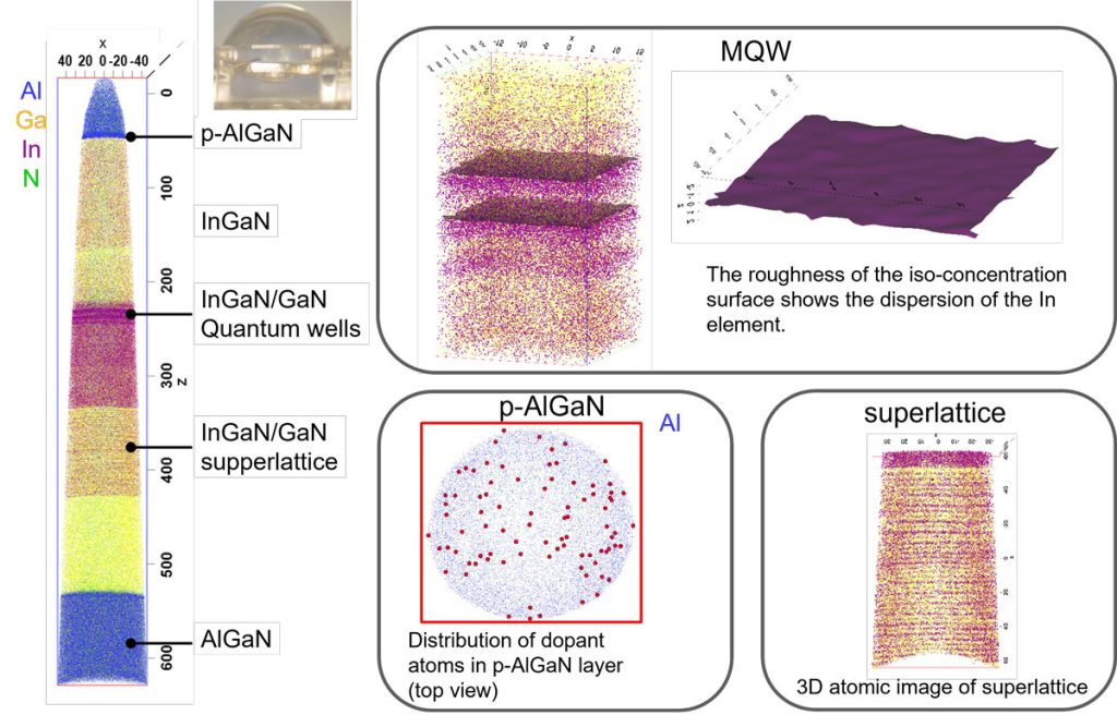
Atom Probe Tomography (APT) is a nanoscale materials analysis technique that provides 3D (three-dimensional) spatial imaging and chemical composition measurements with high sensitivity simultaneously. APT is very useful in providing specific information on segregation of elements along grain boundaries, understanding dopants, nanoscale precipitates, and analysis of light (low mass) elements.
While other techniques can’t identify segregation of elements along grain boundaries, APT is well equipped for this task. During product/process development, this type of analysis can help to determine how a material property is affected which in turn can affect the end product in terms of strength, elasticity and strain. Segregation of elements are also tell-tale signs of fatigue, cracks and aging causing product failure.
Doping is when elements are added to a specific layer. The dopants change the electronic property. However, clustering can occur in the dopants causing it to affect the performance. In semiconductor devices, APT can help verify if doping was done properly during process development while identifying concentration of elements within a small area. The same analysis is helpful in failures when trying to determine contamination.
Lighter elements such as lithium, beryllium, carbon, nitrogen, and oxygen are difficult to analyze in nanoscale using other techniques, but APT can help. For lithium, segregation along the grain boundaries may impede motion in the battery and directly impact how long it will last. For boron used in stainless steel and glasses, segregation can affect strength, fracture or fatigue in that area.
APT is an advanced tool that can provide thorough information during process development and failure analysis. At Eurofins EAG, we invest in new tools and technologies to provide our clients with the best data. We are currently the only commercial laboratory in the US offering Atom Probe Tomography (APT) services, and that is just one of the many techniques and services we have to offer. With our years of expertise, knowledge, and wide range of analytical tools, we partner with our clients to help identify and solve problems.
Contact us today to learn how we can help you on your next project.
For over 40 years, EAG has been involved in the entire glass value chain, from raw starting materials to final products.
In this webinar will be presenting information on scanning Microwave Impedance Microscopy (sMIM) operation.
In this webinar we introduce analytical techniques for the characterization of Li-ion battery electrode (cathode) at different length scale
This webinar will focus on Electron Backscatter Diffraction (EBSD) and Electron channeling contrast imaging (ECCI)
To enable certain features and improve your experience with us, this site stores cookies on your computer. Please click Continue to provide your authorization and permanently remove this message.
To find out more, please see our privacy policy.