Advances in the Semiconductor Industry with Gallium Oxide

As technology advances the attractiveness of being able to travel further, faster and with environmental efficiently increases as well. One aspect which the semiconductor industry can address is power conversion for electric trains and vehicles. Power devices are made from a variety of materials including silicon carbide (SiC) and gallium nitride (GaN). More recent research focuses on the unique properties of gallium oxide (Ga2O3)

What is Gallium Oxide (Ga2O3)?

Gallium oxide (Ga2O3) is a material which has the potential to replace or substitute gallium nitride (GaN) in power conversion devices. One advantage of gallium oxide over gallium nitride (GaN) is its ability to be grown in bulk. Bulk gallium nitride, or even GaN thin films (GaN) tend to form structural defects which affect device performance. Gallium oxide (Ga2O3) can be used at a higher voltage resulting in increased efficiency. Some potential applications could be electric vehicles due to higher voltage transistors (for inverter or converter), electric trains which need super high-powered devices, and other applications outside of power conversion such gas sensors.

Gallium Oxide – Advances in the Semiconductor Industry

There are some challenges with gallium oxide (Ga2O3) that need to be addressed before it can become mainstream. For example, with gallium oxide (Ga2O3) the thermal conductivity is not as good as other materials which may cause a device to overheat.

EAG Offers Wide Range of Materials Testing Techniques for Gallium Oxide (Ga2O3) Analysis

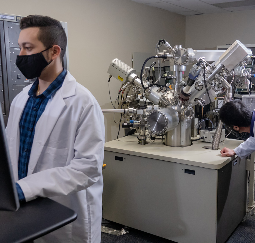
Currently, there are not many companies investigating this material, but that can change quickly with the ever-evolving semiconductor market. When that shift occurs Eurofins EAG Laboratories is ready as we offer a wide selection of techniques which can be used to analyze this material and ensure its safety for use.  EAG scientists can use Transmission Electron Microscopy (TEM), Glow Discharge Mass Spectrometry (GDMS Analysis) and Inductively Coupled Plasma Mass Spectrometry (ICP-MS) to study the material in depth as well as Secondary Ion Mass Spectrometry (SIMS Analysis) to measure the dopant profile of the material and provide imaging to analyze the crystal defect.

As the semiconductor industry continues to grow and evolve EAG will be your partner to make sure your end-product operates well and safely. We are ready to help you with your analyses so contact us today to begin the process.

More content you might like...

GC-MS

GC-MS Webinar

In this webinar we will focus on Gas Chromatography-Mass Spectrometry (GC-MS) which allows for the identification of specific molecules

Read More »

To enable certain features and improve your experience with us, this site stores cookies on your computer. Please click Continue to provide your authorization and permanently remove this message.

To find out more, please see our privacy policy.