Failure Analysis in a Complex World Webinar
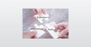
In this webinar we show how EAG troubleshoots electronic system failures using a multidisciplinary approach


In this webinar we show how EAG troubleshoots electronic system failures using a multidisciplinary approach
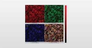
In this webinar we introduce analytical techniques used by EAG for surface analysis – XPS, Auger and TOF-SIMS

Wednesday, May 14, 2025
This webinar will cover the chemical characterization of consumer products using extractable/leachable studies. Register to reserve your spot today!
In this webinar we introduce how a 3rd Party Analytical Lab Can Help Support Your Company’s Compliance with EU’s MDR
To enable certain features and improve your experience with us, this site stores cookies on your computer. Please click Continue to provide your authorization and permanently remove this message.
To find out more, please see our privacy policy.