
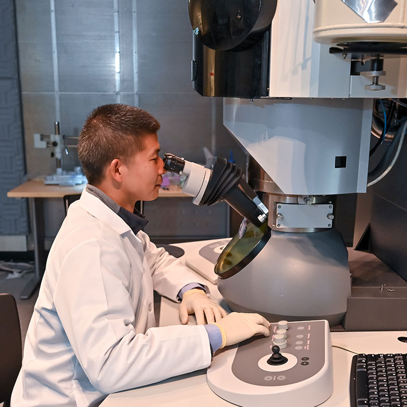
High Detection Sensitivity at the Nanoscale Level – APT
APT is a nanoscale materials analysis technique that provides 3D spatial imaging and chemical composition measurements with high sensitivity simultaneously.
Home » Checking Local Bonding in VCSEL Apertures
VCSELs, or vertical cavity surface emitting lasers, are an essential technology we rely on every day. They can be found in commonplace equipment such as your computer mouse and laser printer, to advanced sensors such as LIDAR or even data storage applications. Although they are increasingly common, their properties are highly tunable and require rigorous development to prepare a reliable and efficient product.
There are many key components of the VCSEL, but one challenging region is the oxide aperture. The oxide aperture is responsible for current confinement, and it is important to have high quality oxidation to prevent failure of the device. Although VCSELs can exhibit failure in many ways, it is important to characterize the failure and determine how it could be prevented in future products. EAG can help!
AC-STEM analysis can provide a visual representation of localized device regions. From atomic structure to local bonding – AC-STEM unlocks key sample features that are important to understand for modern devices. For example, correct oxidation of the VCSEL aperture layer is key.
During the oxidation process, getting the correct layers to oxidize without forming unwanted phases is important. AC-STEM with EELS can be utilized to understand variations in the oxide layer with nanoscale resolution.
AC-STEM imaging is essential towards studying these types of fine sample features because bulk techniques lack the necessary spatial resolution. By combining this type of analysis with other Eurofins EAG services such as SIMS, it is possible to gain a clear understanding of the VCSEL device structure and composition with atomic scale resolution and dopant level composition sensitivity.
Contact us today to learn how we can help you on your next project.

APT is a nanoscale materials analysis technique that provides 3D spatial imaging and chemical composition measurements with high sensitivity simultaneously.

III-V materials partially provide us with the ever evolving and changing technological advances we enjoy today.

FTIR, Raman and NanoIR are particularly well suited at determining the identity and molecular structure of organic materials, however they can also obtain some inorganic information too.
Electrical AFM can measure the electrical/electromechanical properties of various functional materials and samples. This helps distinguish between conductive and nonconductive areas or polar and nonpolar regions of a device.
To enable certain features and improve your experience with us, this site stores cookies on your computer. Please click Continue to provide your authorization and permanently remove this message.
To find out more, please see our privacy policy.