
Elemental Depth Profiling Analysis for the Aerospace & Defense Industry
EAG Scientists utilize GDMS analysis to perform Elemental Depth Profiling for chemical purity evaluations for aerospace & defense.


EAG Scientists utilize GDMS analysis to perform Elemental Depth Profiling for chemical purity evaluations for aerospace & defense.
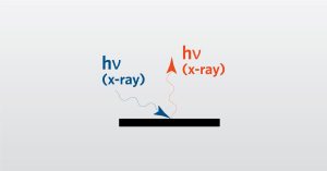
In this webinar we introduce Total Reflection X-ray Fluorescence (TXRF) which is a non-destructive elemental survey technique.
June 27, 2024
During this live Ask the Expert event, we will answer pre-submitted questions from our audience regarding Elemental Analysis with Inductively Coupled Plasma (ICP-OES, ICP-MS, LA-ICP-MS). These techniques provide full survey major, minor, trace element analysis, and purity certification for up to 69 measurable elements.

In the early stages of materials development for consumer electronics, a myriad of technologies comes into play, including semiconductors, MEMs & NAND structures, plastics, glass, and various raw materials.
To enable certain features and improve your experience with us, this site stores cookies on your computer. Please click Continue to provide your authorization and permanently remove this message.
To find out more, please see our privacy policy.