Using SIMS to Scrutinize HEMTs
Home » Using SIMS to Scrutinize HEMTs
From the buffer layer to the very top of the device, a novel form of SIMS can uncover troublesome impurities in GaN-on-silicon HEMTs
One of the devices attracting the most interest in the compound semiconductor manufacturing industry is the GaN-based HEMT (also known as GaN FET). Its capability to operate at high voltages and deliver high powers at microwave frequencies makes it an attractive candidate for deployment in base stations, and in a range of defence applications, including radar.
The impressive performance of this wide bandgap HEMT stems from the specific material properties associated with GaN. Compared to GaAs-based materials, which have also been used for generating power in the microwave region, GaN has a larger peak electron velocity; a higher thermal stability; and a larger band gap. All of these traits make GaN a very appropriate material for the channel of a HEMT. In such structures it is often paired with AlGaN to form a two-dimensional electron gas (2DEG), which lies at the very heart of the device, dictating its electrical characteristics.
Selecting the best substrate for the manufacture of GaN HEMTs is far from easy. From a performance perspective, GaN is ideal, because it ensures a perfect lattice match between the epilayers and the foundation. If such a substrate were practical, it would allow the use of a relatively thin buffer layer, because its role would only be to isolate the 2DEG from the substrate – it would not be needed to prevent high levels of defects in the active region of the device.
But today GaN substrates cannot be grown in sufficiently large sizes to make their price commercially viable. Consequently, GaN HEMTs have to be grown on foreign substrates. One common choice is singlecrystal SiC, which combines good electrical and thermal conductivity with a lattice constant that is close to that of GaN – the difference is just 3 percent. However, while not as expensive as GaN, SiC is still pricey.
A cheaper alternatives is sapphire, but it has a poor thermal conductivity − a disadvantage for high-power devices − and its lattice mismatch with GaN is 13 percent. Due to these drawbacks, a more popular low-cost option is silicon, which is now drawing a great deal of attention. Its great strength is that it has a large base of established manufacturing tools and processes. However, it also has its weaknesses, including a very large lattice mismatch with GaN that gives rise to a high density of defects in the epilayers. To prevent the defect density in the active layers from being so high that device performance is unacceptable, thick AlGaN buffer layers are inserted between the substrate and the 2DEG-forming layers.
Scrutinising the HEMT
A characterisation technique that can reveal a great deal about GaN-on-silicon HEMTs is a variant of secondary ion mass spectrometry known as ‘Pointby- point CORrected’ SIMS, or PCOR-SIMS.
We have developed this at EAG Laboratories. Compared to regular SIMS, it can determine layer thickness, composition and doping profile more accurately, because, at every data point, a calibration is undertaken with respect to alloy composition.
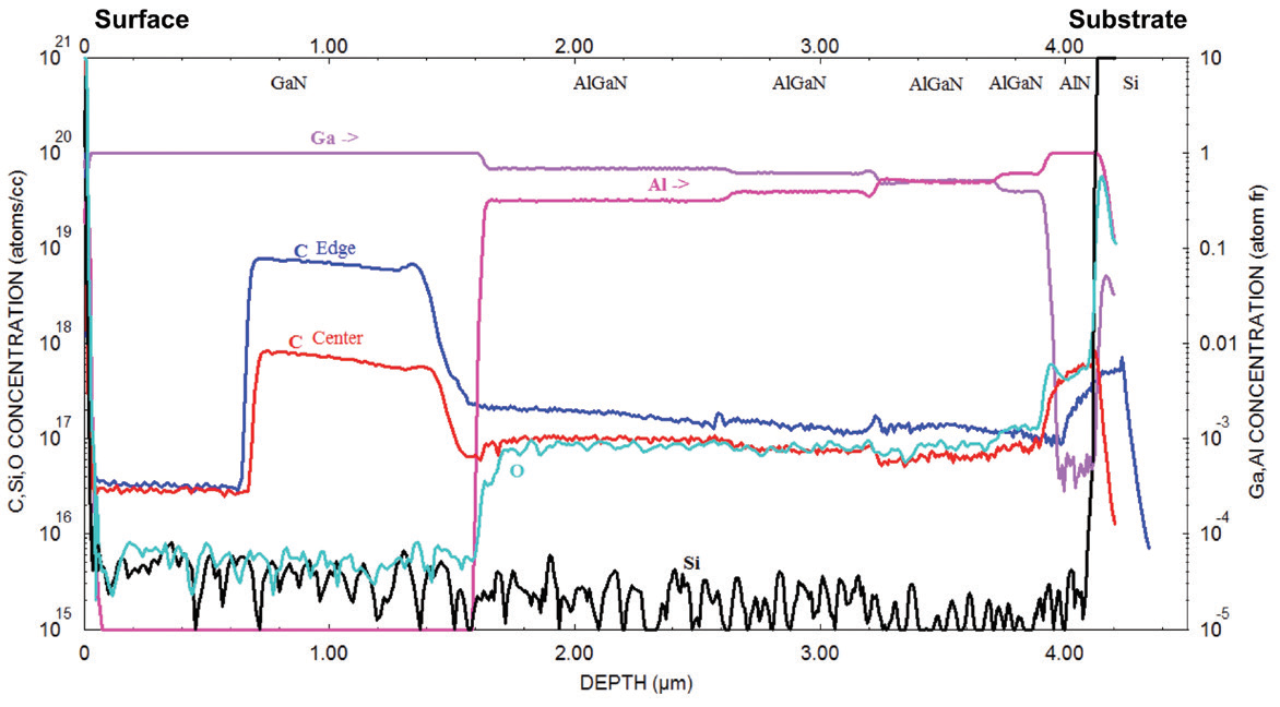
In the remainder of this article, we will take a journey through a GaN HEMT, or GaN FET, grown on 150 mm silicon, beginning with the buffer layer and finishing with the region around the 2DEG (see Figure 1). During this trip we will comment on the influence of pits on device profiling; uncover impurities that can hamper device performance; and understand the composition of the channel of the device.
We start our journey with the buffer layer, which is made of AlN. This material is not well lattice-matched to the underlying silicon, but it serves two important purposes: it provides an insulating layer that isolates those above from the substrate; and it acts as a seed layer, aiding the growth of subsequent layers of AlGaN with successively diminishing aluminium content. By decreasing the proportion of aluminium in AlGaN, the defect density is reduced to acceptable levels for subsequent growth of the GaN barrier.
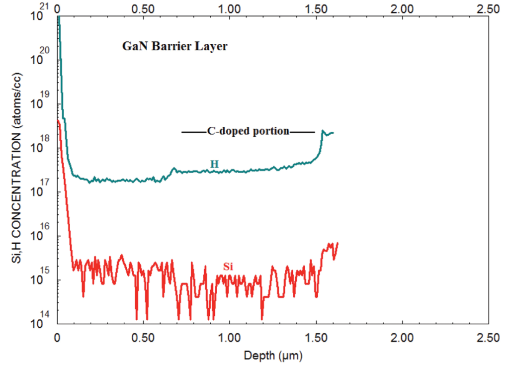
Another insight provided by the PCOR-SIMS profile, shown in Figure 1, is that the bottom half of the GaN barrier layer is doped with carbon. This compensates for unintentional n-type doping by impurities (mainly silicon and oxygen) in the AlGaN buffer, and leads to an increase in the breakdown field strength. Unfortunately, at the edge of the wafer, the carbon doping in the GaN portion of the buffer is ten times higher than it is in the centre (Figure 1). This has considerable implications on the capability of the barrier layer to reduce the electric field, which varies across the 150 mm wafer.
The good news is that at a greater vertical distance above the substrate, where the growth of AlGaN begins, variations in thickness and doping level between the centre and the edge of the wafer are far smaller. It is important to monitor the level of carbon, as well as that of silicon and oxygen, because if carbon is excessively high, it will lead to leakage in the device.
According to reports, carbon doping is a major issue in the vicinity of the 2DEG, because it promotes a vertical leakage current. This is highly undesirable, because it degrades the carrier density and the carrier mobility of the 2DEG channel electrons, leading to an increase in dynamic on-resistance and current collapse. All these changes are to the detriment of device performance and reliability.
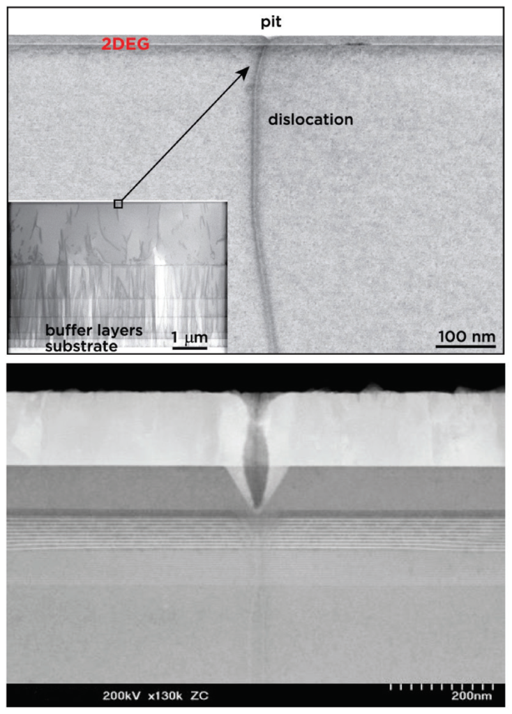
Despite the detrimental character of carbon doping on the 2DEG and the device properties, there are only a few reports that consider the residual carbon level in the active layers (the AlN spike and the AlGaN barrier layer). Perhaps this is because the measurements of carbon in this near-surface region are severely hampered by surface pits, which are always present, due to threading dislocations that originate deep in the buffer layer and reach the surface (see Figure 2).
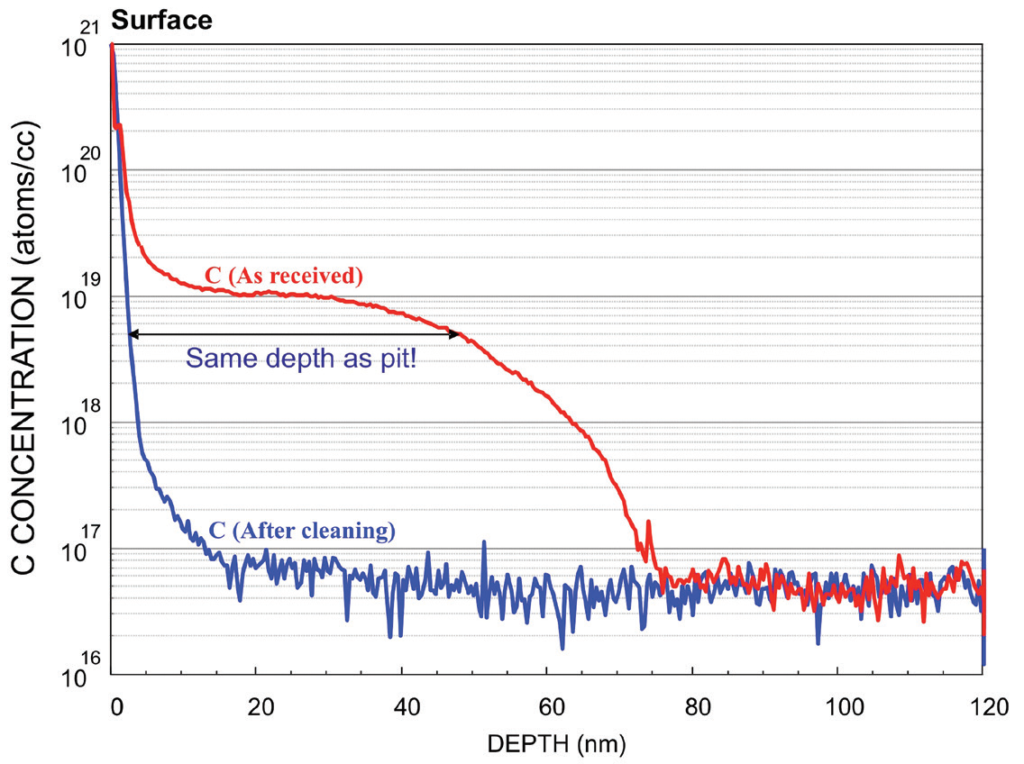
In this region it is not easy to measure the carbon profile accurately. Carbon-containing species are adsorbed onto the air-exposed top surface, and are not entirely removed by the SIMS sputtering process until the entire pit is sputtered through.
This leads to an artificially deep carbon profile, which can totally obscure the real carbon distribution in the 2DEG region.
To circumvent this problem, we have developed a proprietary surface-cleaning procedure that removes the vast majority of carbon from the surface, thus eliminating the deep tail of the carbon profile (see Figure 3).
Thanks to this, true measurements are possible for the carbon concentration in the AlGaN barrier layer just above the 2DEG, as well as in the AlN spike just below it.
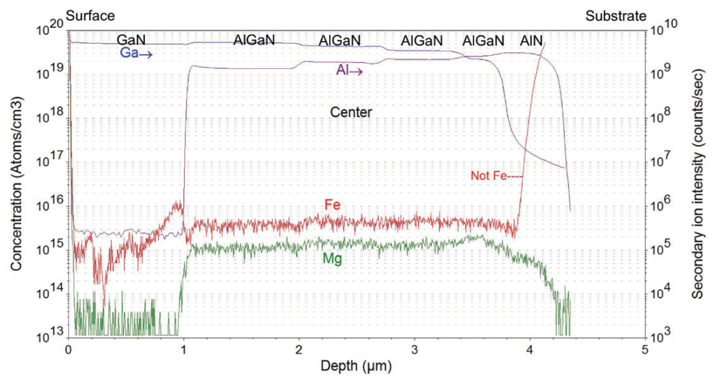
Iron and magnesium can also be used to dope the buffer layer. For these elements, SIMS provides very low detection limits.
This is evident in Figure 4, which shows a peak in the iron profile just inside the GaN barrier. This peak is absent at the edge of the wafer, highlighting another difficultly in growing uniform layers across large substrates.
It is also important to control non-metallic impurities in the GaN barrier layer. The level of silicon in the GaN directly below the 2DEG must be as low as possible, because the device is designed to function in the absence of dopants.
SIMS can be capable of silicon detection limits in the mid 1014 atom/cm3 range, which is low enough to see the troublesome 2 x 10¹⁵atom/cm3 silicon level just beneath the 2DEG in a GaN HEMT (see Figure 5).
Another concern raised by this profile, shown in Figure 5, is the level of hydrogen in the GaN barrier. Hydrogen can have deleterious effects on device reliability, so it is critical to keep its levels as low as possible. In this case, PCOR-SIMS reveals a higher hydrogen-level in the carbon-doped portion of the barrier that is lightly elevated in carbon content. Presumably, this arises from the precursor used for carbon doping.
To the 2DEG
Near the surface of the structure is the twodimensional electron gas, which is responsible for current flow in the transistor. This 2DEG results from a conduction-band discontinuity between a thin, top, doped AlGaN layer and an undoped GaN layer.
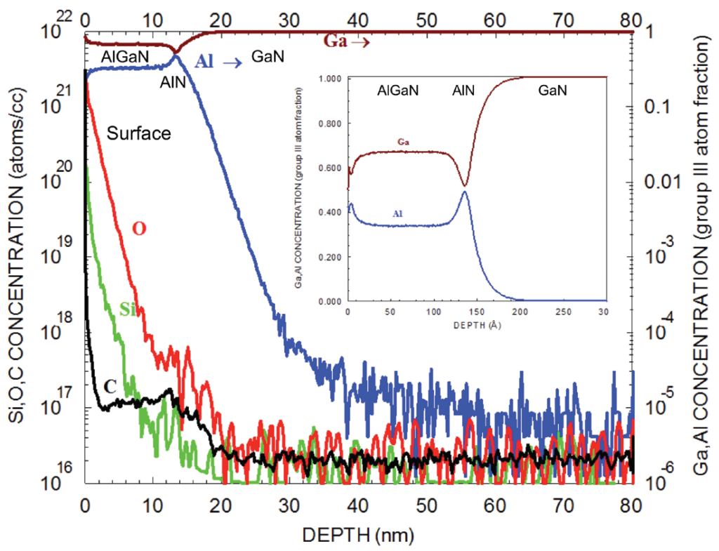
This creates a triangular quantum well that accumulates electrons. The active region is exceedingly thin, with a thickness of just 20-30 nm. Consequently, measuring this accurately by SIMS requires great care. However, with PCOR-SIMS, it is possible to identify the aluminium level in the top AlGaN layer, as well as the impurity levels of carbon, hydrogen, oxygen and silicon (see Figure 6).
Since this AlGaN layer is on the top of the structure, it is important to take steps to minimize the effects of surface contamination, which is always present on air-exposed surfaces. To achieve this, we use our proprietary surface-cleaning procedure to remove the carbon initially present on the sample surface. This enables a determination of the carbon doping level in the AlGaN layer of 1-2×10¹⁷ atoms/cm3, within the top 15 nm of the sample.
This particular measurement also yields another important piece of information for the device engineer – the thickness of the AlGaN barrier layer (see the inset to Figure 6).
It is through this layer that the potential on the gate acts to control the electron density in the 2DEG, and thus the conductance of the device.
Another way to look at this region is to overlay the profiles of aluminium and carbon on a cross-sectional transmission electron microscopy image of the same region (see Figure 7). With this approach, it is possible to see the location of the AlN delta layer. Its role is to improve the carrier mobility in the 2DEG, by mitigating coulomb scattering from donors in the AlGaN. The micrograph reveals that the actual thickness of the AlN delta layer is correctly measured by the full-width-half maximum of the aluminium profile above the constant level in the AlGaN layer. However, there is a tail into the underlying GaN, due to surface pits (shown in Figure 3). A plot of the carbon concentration reveals the location of the doping with respect to the exact vertical location of the interface, which is shown by the aluminium profile. Note that transmission electron microscopy cannot be used to detect carbon, even with energy dispersive X-ray spectrometry or electron energy-loss spectroscopy.
Also shown in Figure 7 is a plot of conductivity. This is influenced by the instantaneous surface potential, from which can be inferred the surface conductivity.
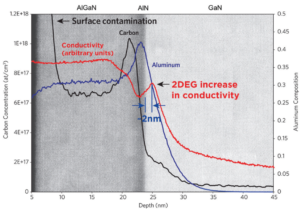
The 2DEG is formed just inside the GaN, at the depth at which sample conductivity recovers after passing through a zone of decreased conductivity, just inside the barrier layer where the holes accumulate. Our study of the HEMT, from the buffer to the 2DEG, show the tremendous capability that PCOR-SIMS has for determining accurate concentrations of matrix elements and dopants within GaN HEMTs. This technique can be used to optimise epitaxial layer growth, aid failure analysis, and thus support the growth of the GaN HEMT (GaN FET) industry.
Would you like to learn more about Using SIMS to Scrutinize HEMTs?
Contact us today for using SIMS to scrutinize HEMTs. Please complete the form below to have an EAG expert contact you.