Semiconductor Stress Measurements by Raman Spectroscopy
Home » Semiconductor Stress Measurements by Raman Spectroscopy
Stress control in silicon and other semiconductor devices is of primary importance in order to prevent problems related to the nucleation and propagation of dislocations and the formation of cracks and voids.
The sources of the strain developed in devices during or after processing are different in nature. They might result due to thermal processes, embedded structures, such as trenches, or non-planar growth of field oxides.
Measuring stresses by a nondestructive technique, with good spatial resolution is achieved successfully by Raman spectroscopy. Mechanical stress causes frequency shifts in Raman modes (phonons). The magnitude of the frequency shift is proportionally related to the strain developed, though the measurement of all strain tensor components is not straightforward.
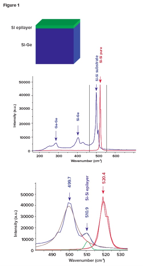
This application note describes the measurement of the stress developed in a thin Si epilayer (~0.1-0.2 µm thick) grown above a SiGe substrate with 30% Ge in it (Figure 1).
The penetration depth of a 514.5 nm wavelength laser beam is ~0.8 µm, so the Raman spectrum (blue) has spectral contributions from both the epilayer and the substrate. The SiGe Raman spectrum has three peaks corresponding to vibrations of Ge-Ge, Si-Ge and Si-Si atoms, respectively. A weak peak appears on the shoulder of the substrate Si-Si vibration (499.9 cm-1) due to the Si epilayer phonon (510.9 cm-1).
The Si epilayer Raman wavenumber is red-shifted (~9.5 cm-1) from the Si vibration of a stress free silicon sample (red spectrum). This red-shift demonstrates a tensile strain in the Si epilayer caused by the difference in lattice parameters of Ge and Si.
If a biaxial stress is supposed in the silicon epilayer, each component of the tensile stress is calculated to be ~2.4 Giga Pascals (Gpa).
Would you like to learn more about Semiconductor Stress Measurements by Raman?
Contact us today for your semiconductor stress measurements by Raman. Please complete the form below to have an EAG expert contact you.