Depth Profile Characterization of Low-K Materials Using SIMS
Home » Depth Profile Characterization of Low-K Materials Using Secondary Ion Mass Spectrometry
Depth profile characterization of low-k materials assists in the continually shrinking dimensions of integrated circuits. These shrinking geometries bring new challenges for materials characterization.
The use of Cu instead of Al for interconnects in silicon devices and the use of low-K dielectric materials to replace SiO2 have led to significant advances in IC speed and performance, but also to complications with materials processing and integration.
SIMS is one of the most valuable techniques for characterizing insulating, semiconductor, and metallic materials and can help solve process and integration problems. However, low-K dielectric materials introduce new issues for SIMS depth profiling. The unique insulating properties, chemical structure and often porous nature of the H or C-rich low-K materials make SIMS analysis very challenging since the analysis itself can degrade the material.
Low-K films are made in a wide spectrum of compositions and there is usually no standard sample available for SIMS data quantification. At EAG Laboratories, we have solved these issues.
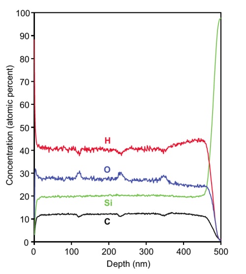
Figure 1 shows a SIMS profile of a porous organosilicate low-K film. From this measurement we can get the atomic percent of H, C, O, and Si as a function of depth. Periodic peaks and dips in the profile show interfaces in this multi-layer structure.
EAG can provide depth profile characterization services, including:
- Measurements of the H, C, O, and Si depth profiles with minimal damage to the sample from the analysis.
- Improved impurity analyses, such as F, N, Cl, and other metal elements.
- Accurate quantification for all measured species and matrix using our unique reference materials.
Would you like to learn more about Characterization of Low-K Materials Using SIMS?
Contact us today for your characterization of Low-K material needs. Please complete the form below to have an EAG expert contact you.