Automatic Critical Dimension Measurements Enabled by Deep Learning
Home » Automatic Critical Dimension Measurements Enabled by Deep Learning
Deep learning methods for image segmentation enable accurate critical dimension measurements from images with complex contrast patterns.
Critical dimension measurements are a key part of micro- and nano-scale solid state device characterization. Whether it is an electronic device in a semiconductor chip or a nanopore for DNA sequencing, critical dimensions often determine the overall performance and yield of the device during manufacturing. Utilizing image processing to analyze microscopy images is a common method for automatically performing critical dimension measurements. Transmission electron microscopy (TEM) is the primary tool used to image devices when nanoscale spatial resolution is required. However, there are a variety of mechanisms that generate contrast in TEM images, including diffraction, chemical composition, sample thickness, zone-axis alignment, and image defocus, all of which combine to generate the final image. This can make it very difficult to write a metrology recipe to automate critical dimension measurements using only conventional image processing. Although scanning transmission electron microscopy and spectroscopy techniques may provide signals that are easier to interpret or process, their acquisition speeds are significantly slower than regular TEM imaging. These issues and trade-offs are not unique to TEM; similar complexities can affect scanning electron microscopy and optical microscopy as well.
In this application note, we highlight how deep learning methods for image segmentation, such as convolutional neural networks (CNNs) or vision transformers, can help interpret the complex contrast of TEM images and segment a series of thin films in 3D NAND devices. Download the application note to learn more.
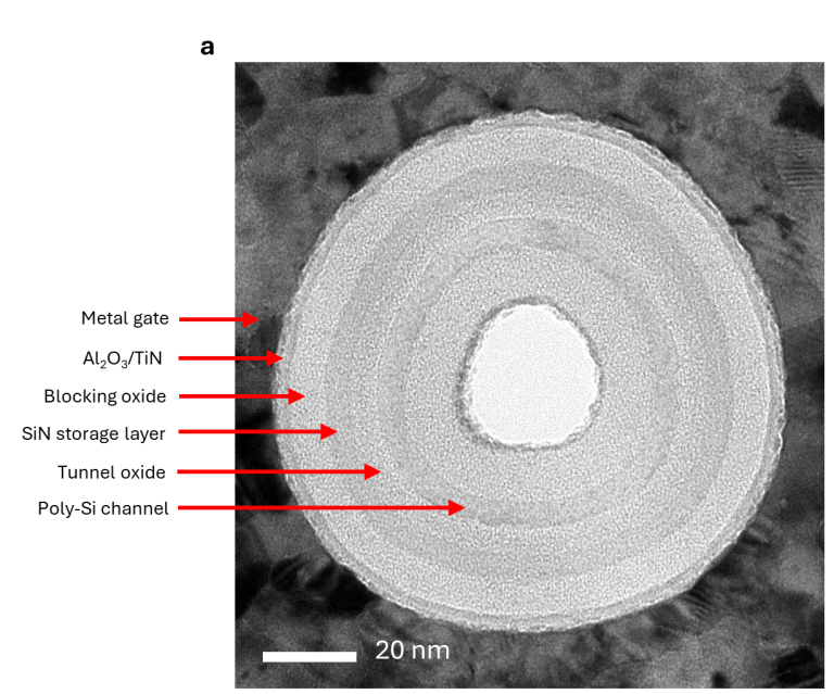
Top image – TEM image of a 3D NAND structure from a planview lamella.
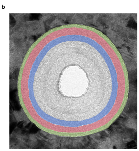
Bottom image – Segmentation masks for the Al2O3/TiN (green), blocking oxide (red), and nitride storage (blue) layers generated by the vision transformer model.
Would you like to learn more about TEM?
Contact us today for your needs. Please complete the form below to have an EAG expert contact you.