Applications of 4D-STEM in Materials Characterization
Home » Applications of 4D-STEM in Materials Characterization
Measuring nanoscale structural and electrostatic properties
of materials using 4D-STEM.
Scanning transmission electron microscopy (STEM) is an essential tool in materials characterization providing both high resolution imaging and spectroscopy when coupled with energy-dispersive x-ray and electron energy loss detectors. During regular STEM imaging, a diffraction pattern from the converged probe is projected onto detectors below the sample and images are constructed by integrating large portions of the diffraction pattern to generate one intensity value per probe position; the image is constructed one pixel at a time by raster scanning the probe across the sample. This integration process discards vast amounts of information contained in the diffraction pattern about the sample’s structural and electrostatic properties. However, the development of fast cameras synchronized with the scanning probe has led to the wide adoption of four-dimensional STEM (4D-STEM), where a diffraction pattern is captured for every probe position in the raster scan. This allows us to capture all the information available from the probe’s interaction with the sample and then use computational analysis to measure the sample’s properties. This process is illustrated schematically in Figure 1.
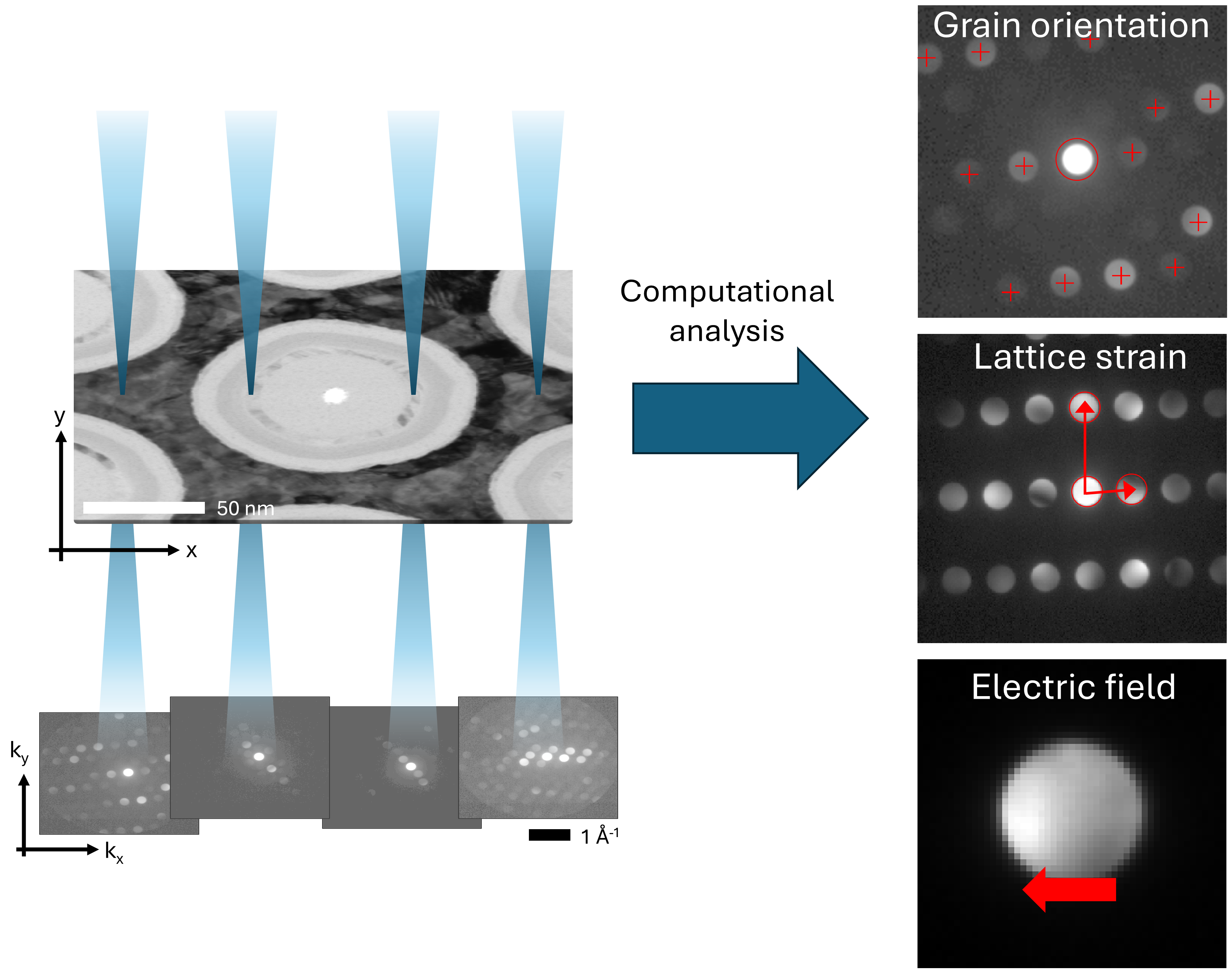
In this application note, we will focus on three applications of 4D-STEM: orientation mapping, strain analysis, and electric field imaging. Download the application note to learn more.
Would you like to learn more about 4D-STEM?
Contact us today for your materials characterization needs. Please complete the form below to have an EAG expert contact you.