Advancing Semiconductor Failure Analysis: Eurofins EAG’s Plasma FIB Delayering
Home » Advancing Semiconductor Failure Analysis: Eurofins EAG’s Plasma FIB Delayering
As semiconductor technology evolves, modern devices are designed with enhanced performance and capabilities, featuring more process layers, denser layouts, intricate circuitry, and highly sensitive gate structures—all within shrinking architectures. The growing structural complexity and shrinking feature dimensions of modern devices make identifying and analyzing defects and failures, whether introduced during manufacturing or arising from use, significantly more challenging during failure analysis.
An important physical failure analysis technique for imaging failure mechanisms on a die is deprocessing, also known as delayering. This process involves the controlled removal and exposure of each individual FAB process layer for detailed inspection. However, traditional chemical and mechanical polishing methods used for older, larger semiconductor nodes are no longer viable for the newer generation of technologies, which feature thinner, smaller, and more complex structures.
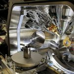
At Eurofins EAG Laboratories, we have utilized Plasma Focused Ion Beam (PFIB) to overcome the limitations of traditional deprocessing methods. By leveraging the advanced capabilities of a modern PFIB, we can perform precise, planar removal of individual process layers across large surface areas, even on leading-edge geometry nodes. This approach not only allows our engineers to perform consistent and controlled in-situ inspection of each process layer, but also facilitates other advanced, analytical techniques such as voltage contrast, EBIC/EBAC/EBIRCH, and nanoprobing.
Would you like to learn more about plasma FIB delayering?
Contact us today for your quality of metal powder feedstocks needs. Please complete the form below to have an EAG expert contact you.
