Aberration Corrected Scanning Transmission Electron Microscopy (AC-STEM) Services
Home » Aberration Corrected Scanning Transmission Electron Microscopy (AC-STEM) Services
Aberration Corrected Scanning Transmission Electron Microscopy (AC-STEM) is the next generation of imaging tools capable of providing information at the Angstrom scale. EAG is proud to be the first independent analytical lab to provide AC-STEM capabilities to its customers. AC-STEM significantly improves the resolution of the traditional STEM tools, providing resolution of better than 0.14 nm on our Hitachi HD2700.
The improvement in resolution and sensitivity that AC-STEM provides is universally applicable for investigations of nanometer scale materials. We specialize in studies involving ultrathin films, nanoparticles, complex interfaces, multiphase materials, interlayer mixing, grain boundary engineering, and surface phenomena.
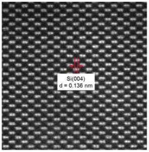
Figure 1 shows the Z-Contrast image of silicon dumbells. The bright spheres are columns of silicon atoms with a spacing of 0.136nm, highlighting the outstanding image resolution of the technique.
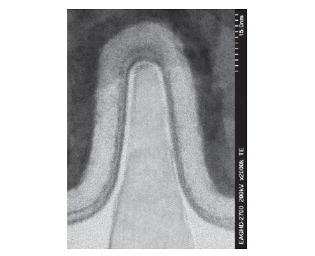
Figure 2 is a high resolution BF STEM image and below is an associated composite elemental map showing the structure of a FinFET device with single-nm scale process layers.

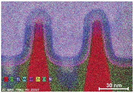
Figure 3 shows a STEM-EDS map of FinFET structure. The elemental maps can have a resolution of ~1nm and detection limit of ~1%. EDS is an excellent method for creating multielement maps, linescans and spectra for a variety of analysis types, including process development, defect analysis and reverse engineering.


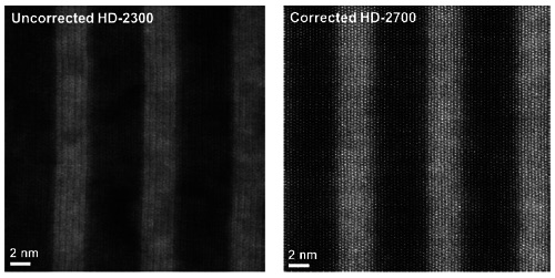
Figure 4 shows a comparison of standard STEM and AC-STEM using the same family of tools. Notice several factors:
- Overall resolution is better in the AC-STEM image. The atomic columns are clearly resolved in the AC-STEM image and less clearly resolved in the uncorrected data.
- The uncorrected image shows slightly more beam damage than the AC-STEM image. This beam damage appears as a general cloudiness in the uncorrected image.
Summary of Aberration Corrected Scanning Transmission Electron Microscopy (AC-STEM) Services
The Materials Sciences division of EAG Laboratories is the leading global provider of surface analysis and materials characterization services. We combine state-of-the art equipment and microscopy experts, experienced in working with advanced materials and high tech products, to ensure the highest quality imaging results. We understand that the newest generation of STEM technology can only be coupled with the newest generation of sample preparation tools to create exemplary images. We look forward to tackling your toughest materials problems.
Would you like to learn more about AC-STEM?
Contact us today for your Aberration Corrected STEM needs. Please complete the form below to have an EAG expert contact you.