Santa Clara, CA
Home » About Us » Locations » North America » Santa Clara, CA
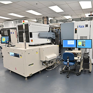
Located in the heart of Silicon Valley, this 45,000 sq. ft. laboratory was built in 2009, and was previously known as EAG’s Microelectronics Test and Engineering (MTE) division. Our Santa Clara location offers semiconductor and microelectronics services, ATE production test and development, burn in and reliability qualification, ESD testing and latch up testing and PCB design and assembly to support new product development, debug and ongoing production. Custom engineering and turnkey, managed projects are a key part of the integrated support model offered.
EAG Laboratories
2710 Walsh Ave.
Santa Clara, CA 95051

Globally serving customers
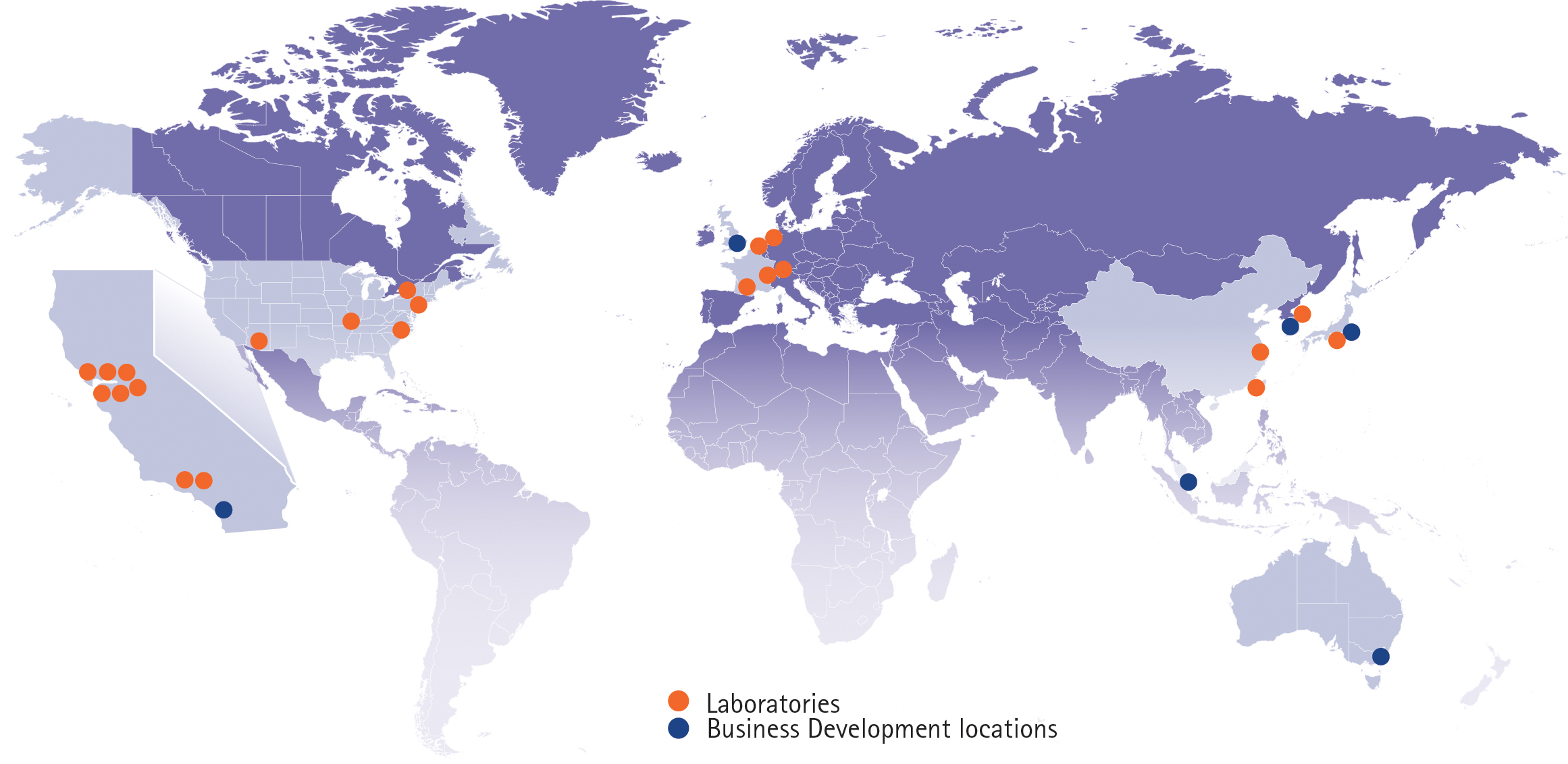
EAG Laboratories offers our clients an extensive knowledge base and skilled expertise that is supported by over 2,500 instruments installed worldwide. This capacity allows us to scale with your demand and time constraints.
We use a centralized support network that gives you access to technical consultants who can discuss every technique or solution that we offer.
